Polycrystalline silicon film solar cell with electric circuit openings

A polysilicon thin film and solar cell technology, applied in circuits, photovoltaic power generation, electrical components, etc., can solve problems such as high manufacturing costs, affect battery performance, and reduce battery efficiency, so as to improve performance and reduce manufacturing costs.

Inactive Publication Date: 2014-01-01
ZNSHINE PV TECH
View PDF0 Cites 0 Cited by
  • Summary
  • Abstract
  • Description
  • Claims
  • Application Information

AI Technical Summary

Problems solved by technology

If a high-purity, high-quality single-crystal silicon wafer is used as the substrate material, the manufacturing cost is extremely high, and if a cheap substrate is used, the impurities in the substrate will easily diffuse into the film, which will easily affect the performance of the battery and reduce the efficiency of the battery.

Method used


Image

  • Polycrystalline silicon film solar cell with electric circuit openings

Examples


Embodiment Construction

[0012] The present invention is described in further detail now in conjunction with accompanying drawing. The drawings are all simplified schematic diagrams, and only illustrate the basic structure of the present invention in a schematic manner, so they only show the configurations related to the present invention.

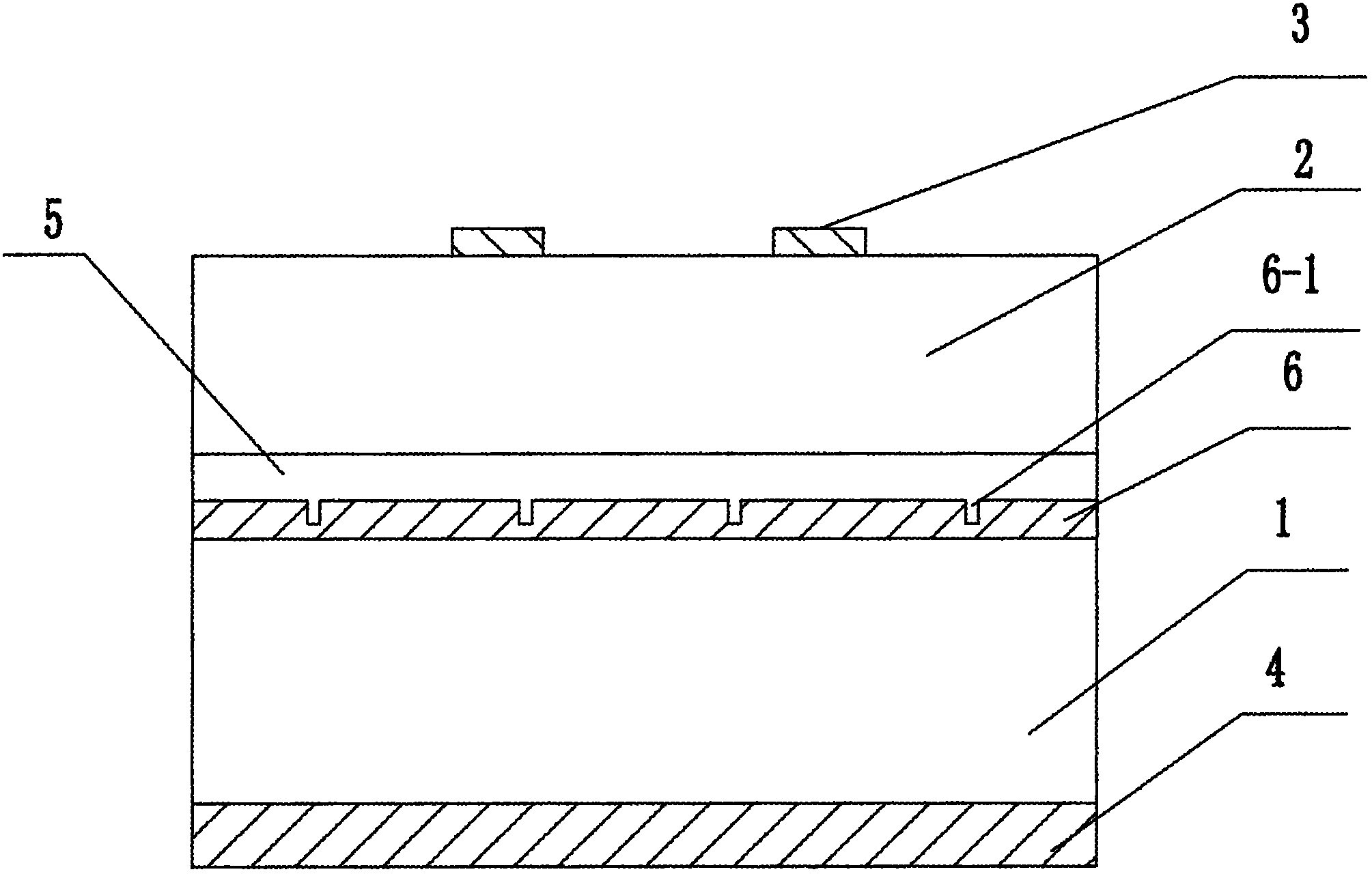
[0013] Such as figure 1 A polysilicon thin-film solar cell with electrical circuit openings shown includes a substrate 1, a polysilicon thin film 2, an upper electrode 3 and a back electrode 4, a p-n junction is formed on the polysilicon thin film 2, and the substrate 1 is arranged on the back electrode 4 A heavily doped P+ layer 5 and a silicon dioxide isolation layer 6 are arranged between the substrate 1 and the polysilicon film 2, and several electrical circuit openings formed by the back electrode 4 and the upper electrode are arranged on the silicon dioxide isolation layer 6. 6-1.

[0014] The thickness of the silicon dioxide isolation layer 6 is 2 microns...


PUM


Abstract

The invention relates to a polycrystalline silicon film solar cell with electric circuit openings. The solar cell solves the problems that an existing substrate is high in price, and impurities in the substrate poor in quality diffuse to a film to affect the quality of the cell. The polycrystalline silicon film solar cell comprises a substrate, a polycrystalline silicon film, upper electrodes and back electrodes, wherein p-n junctions are manufactured on the polycrystalline silicon film, the substrate is arranged on the back electrodes, a heavily doped P+ layer and a silicon dioxide isolating layer are arranged between the substrate and the polycrystalline silicon film, and the electric circuit openings formed by the back electrodes and the upper electrodes are formed in the silicon dioxide isolating layer. The openings are formed in the silicon dioxide isolating layer in a photoetching mode, therefore, the electrodes can be arranged on the front face and the back face of the cell, and manufacturing process of the cell is simplified; the heavily doped P+ layer and the silicon dioxide isolating layer are arranged between the substrate and the polycrystalline silicon film, therefore, a polycrystalline silicon wafer substrate poor in quality can also be used as base material, and manufacturing cost is greatly reduced.

Description

technical field [0001] The invention relates to a silicon solar cell, in particular to a polycrystalline silicon thin film solar cell with an electrical circuit opening. Background technique [0002] Polycrystalline silicon thin-film solar cells are considered to be the best possible replacement for conventional solar cells due to their potential for high efficiency and the dual advantages of forming electrical circuit openings. It has aroused great interest and obtained extensive research in the past ten years. The research is mainly in two aspects: one is the choice of battery substrate, and the other is the preparation process. If a high-purity, high-quality single crystal silicon wafer is used as the substrate material, the manufacturing cost is extremely high, and if a cheap substrate is used, the impurities in the substrate will easily diffuse into the film, which will easily affect the performance of the battery and reduce the efficiency of the battery. Contents of...

Claims


Application Information

Patent Timeline
Patent Type & Authority Applications(China)
IPC IPC(8): H01L31/0352
CPCH01L31/02167H01L31/0352Y02E10/50
Inventor 王桂奋谢德兵王迎春
Owner ZNSHINE PV TECH
Why Eureka
Try Eureka