Lead arc-forming method for manufacturing salient point by utilizing laser

A lead and arc forming technology, used in manufacturing tools, laser welding equipment, semiconductor/solid-state device manufacturing, etc., can solve problems such as reducing efficiency and yield, affecting chip consistency, and inconsistent lead forming, achieving shortened time, Reduce lead damage and ensure consistency

Active Publication Date: 2014-01-08
CENT SOUTH UNIV
View PDF10 Cites 7 Cited by
  • Summary
  • Abstract
  • Description
  • Claims
  • Application Information

AI Technical Summary

Problems solved by technology

The problem with this type of lead forming patent is that in the process of repeatedly bending the lead, it is easy to damage the neck of the lead and even cause the lead to break
The problem with this type of patent is that the complicated trajectory of the riving knife greatly reduces the efficiency and yield
But the problem is that the lead is prone to damage under the action of tools, and the shape of the lead is inconsistent under the action of mechanical force, which greatly affects the consistency of the chip, which is fatal to electronic products

Method used


Image

  • Lead arc-forming method for manufacturing salient point by utilizing laser
  • Lead arc-forming method for manufacturing salient point by utilizing laser
  • Lead arc-forming method for manufacturing salient point by utilizing laser

Examples


example 1

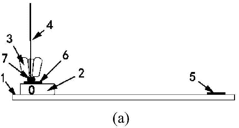
[0045] The method of the present invention is used to form a large-span low-arc lead, such as image 3 As shown, the specific method is:

[0046] Step 1: Form the first solder joint at the midpoint position O of the chip pad (6), such as image 3 as shown in (a);

[0047] Step 2: The rivet rises vertically to point E, releasing a section of lead wire OE, and the length of OE is 7500 microns;

[0048] Step 3: Use the left laser set on the left side of the rivet to irradiate points B and D of the lead from the left side of the rivet respectively, where the OB length is 3000 microns and the OD length is 6750 microns, forming two thermoplastic regions with Large deformation on the left and small deformation on the right form two inflection points protruding to the right; similarly, through the right laser set on the right side of the rivet, the points A and C of the lead wire are irradiated from the right side of the rivet. Among them, the length of OA is 100 microns, and the l...

example 2

[0051] Adopt the method of the present invention to form basic leads, such as Figure 4 As shown, the specific method is:

[0052] Step 1: Form the first solder joint 7 at the center point position O of the chip pad 6, such as Figure 4 (a);

[0053] Step 2: The rivet 5 rises vertically to point E, and releases a section of lead wire 6, the length of which is OE, and the length of OE is 1300 microns;

[0054] Step 3: Use the left laser set on the left side of the rivet to irradiate the point A of the lead wire from the left side of the rivet. The length of the OA is 150 microns to form a thermoplastic zone, which has the characteristics of large deformation on the right and small deformation on the left to form 1 vertices that protrude to the left, such as Figure 4 as shown in (b);

[0055] Step 4: Take point O as the center point, and the distance |OF| between point O and point F is the minor axis of the ellipse. The length of OF is 1000 microns, and the major axis of th...

example 3

[0057] The forming method of the large-span n-arc lead mentioned in the present invention will be based on Figure 5 to describe. The specific method is:

[0058] Step 1: Form the first solder joint at the midpoint position O of the chip pad (6), such as Figure 5 as shown in (a);

[0059] Step 2: The rivet 5 rises vertically to point E, and releases a section of lead wire 6, the length of which is OE, and the length of OE is 5000 microns;

[0060] Step 3: Irradiate point A and point D of the lead wire from the left side of the rivet with the left laser set on the left side of the rivet respectively, where the OA length is 150 microns and the OD length is 4000 microns, each forming a thermoplastic zone , which has the characteristics of large deformation on the right side and small deformation on the left side, so as to form two vertices protruding to the left, such as Figure 5 as shown in (b);

[0061] Step 4: Take point O as the center point, and the distance |OF| betw...


PUM

PropertyMeasurementUnit
lengthaaaaaaaaaa
lengthaaaaaaaaaa

Abstract

The invention discloses a lead arc-forming method for manufacturing a salient point by utilizing laser. The method comprises the steps that step 1, a first welding point is formed in the central position point O of a chip welding pad (6); step 2, a chopper is vertically lifted to a point E, and a lead is released simultaneously; step 3, a point A is at least selected between the point O and the point E of the lead; laser energy is introduced to manufacture a local thermoplastic deformation point for the selected point to form a salient point; step 4, the distance, namely the absolute value of OF, between the point O and a point F is used as the minor axis of an ellipse, the major axis of the ellipse is 4000-8000 micrometer, the chopper moves to the point F from the point E along the elliptical orbit, under the combined action of heat and ultrasound applying on the chopper, a second welding point is formed in the midpoint position F of a frame welding pad (5), and a required large-span low-arc lead is formed. With the implementation of the lead arc-forming method, the movement trail of the chopper is greatly simplified, and the large-span low-arc lead is formed.

Description

technical field [0001] The invention relates to a method for interconnecting wires of microelectronic packaging in semiconductor manufacturing, in particular to a rapid wire forming method for manufacturing one or more inflection points on wires by using laser to form large-span low-arc wires in three-dimensional stacked packaging. Background technique [0002] Integrated circuit manufacturing is one of the core industries of high technology. In order to meet the challenges of smaller size and stronger functions, the integration level of IC has increased, and the characteristic line width has been reduced to below 28nm, which is gradually approaching the physical limit. The industry believes that one of the more effective solutions is a system-in-package (System in Package, SiP) technology. According to the definition of ITRS2010, SiP is an advanced packaging technology that assembles multiple active / passive / MEMS / biological chips and other devices with different functions i...

Claims


Application Information

Patent Timeline
Patent Type & Authority Applications(China)
IPC IPC(8): H01L21/60
CPCH01L24/78H01L24/85B21D11/20B23K26/0093H01L24/43H01L2224/78H01L2224/85H01L2924/12042H01L2224/85205H01L2224/85207H01L2224/78301H01L2924/00H01L2924/00012
Inventor 王福亮陈云韩雷李军辉
Owner CENT SOUTH UNIV
Why Eureka
Try Eureka