Micro-strip-to-waveguide vertical transition structure achieved through multi-layer step type substrate integration waveguide

A substrate-integrated waveguide and integrated waveguide technology, applied in the field of millimeter wave communication, can solve the problems of limited planar circuits and incompatibility of microstrip structures, and achieve the effect of realizing broadband performance and benefiting planar integration

Active Publication Date: 2014-01-15
NO 55 INST CHINA ELECTRONIC SCI & TECHNOLOGYGROUP CO LTD
View PDF2 Cites 38 Cited by
  • Summary
  • Abstract
  • Description
  • Claims
  • Application Information

AI Technical Summary

Problems solved by technology

In recent years, there have also been research reports on the vertical transition from SIW to waveguide, which eliminates the short-circuit surface, and the working bandwidth can be wide or narrow. It is easy to obtain a wider working bandwidth by using the vertical transition of a thicker SIW structure, but such a structure is too thick. The thickness of the substrate is not compatible with the microstrip structure working in this frequency band, which also limits its interconnection with planar circuits, especially functional modules containing active devices

Method used


Image

  • Micro-strip-to-waveguide vertical transition structure achieved through multi-layer step type substrate integration waveguide
  • Micro-strip-to-waveguide vertical transition structure achieved through multi-layer step type substrate integration waveguide
  • Micro-strip-to-waveguide vertical transition structure achieved through multi-layer step type substrate integration waveguide

Examples


Embodiment Construction

[0015] The present invention will be further described below in conjunction with the accompanying drawings and specific embodiments. The following descriptions are only preferred embodiments of the present invention, and it should be pointed out that for those of ordinary skill in the art, without departing from the principle of the present invention, some design and structure improvements and preparation method modifications can also be made. And retouching should also be regarded as the protection scope of the present invention.

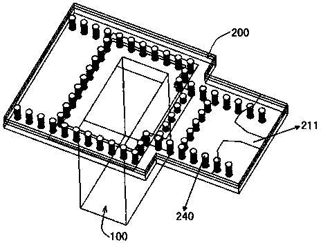
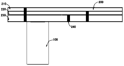
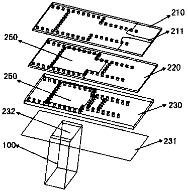
[0016] A multi-layer stepped substrate integrated waveguide realizes the vertical transition structure from microstrip to waveguide, which includes a stepped integrated waveguide structure and a rectangular waveguide. The stepped integrated waveguide structure includes a first substrate, a second substrate, and a third substrate stacked sequentially from top to bottom, and each layer of substrates is provided with an array of metallized through hol...


PUM


Abstract

The invention discloses a micro-strip-to-waveguide vertical transition structure achieved through multi-layer step type substrate integration waveguide. One section of multi-layer step substrate integration waveguide is adopted through the structure to achieve the vertical transition of a micro-strip and a caliber of the waveguide between the micro-strip and the caliber of the waveguide. Coupling calibers are etched among all layers of step substrate integration waveguide and between the substrate integration waveguide at the lowest layer and the caliber of the waveguide, the multi-layer substrate integration waveguide in the two plane directions is in matched connection with the single-layer micro-strip through the step structure, and the broadband performance is achieved. The novel multi-layer step substrate integration waveguide structure is adopted, the short circuit plane is omitted, the plane integration is facilitated, and especially connection between a plane circuit and a waveguide structure system is facilitated. The broadband performance is achieved by optimizing the design calculation.

Description

technical field [0001] The invention belongs to the field of millimeter wave communication, and in particular relates to a vertical transition design technology from a millimeter wave broadband microstrip to a waveguide. Background technique [0002] Microstrip-waveguide transition is widely used in various microwave and millimeter wave modules to realize the transmission of microwave and millimeter wave signals from planar circuits, especially planar integrated circuits containing active devices, to waveguide structures, and waveguide structures are characterized by their Features such as low loss and high Q value are widely used in the millimeter wave frequency band. [0003] So far, traditional microstrip-to-waveguide vertical transitions mainly include E-plane probe-fed type, slot-coupled patch type, and aperture (ground) coupled (stacked) patch type. The former usually requires a short-circuit surface, which is an obstacle to the compactness and integration of the circ...

Claims


Application Information

Patent Timeline
Patent Type & Authority Applications(China)
IPC IPC(8): H01P5/00H01P5/08
Inventor 戴新峰周明
Owner NO 55 INST CHINA ELECTRONIC SCI & TECHNOLOGYGROUP CO LTD
Why Eureka
Try Eureka