Defect detection device for OLED

A defect detection and detection device technology, applied in the direction of single semiconductor device testing, etc., can solve problems such as mass production, and achieve the effects of ensuring the quality of inspection, reducing fatigue, and improving work efficiency

Inactive Publication Date: 2014-01-22
SICHUAN CCO DISPLAY TECH
View PDF5 Cites 12 Cited by
  • Summary
  • Abstract
  • Description
  • Claims
  • Application Information

AI Technical Summary

Problems solved by technology

[0004] In order to solve the mass production problem of the back-end detection process of the existi

Method used


Image

  • Defect detection device for OLED

Examples


Embodiment Construction

[0015] The present invention will be further described below in conjunction with the accompanying drawings and specific embodiments.

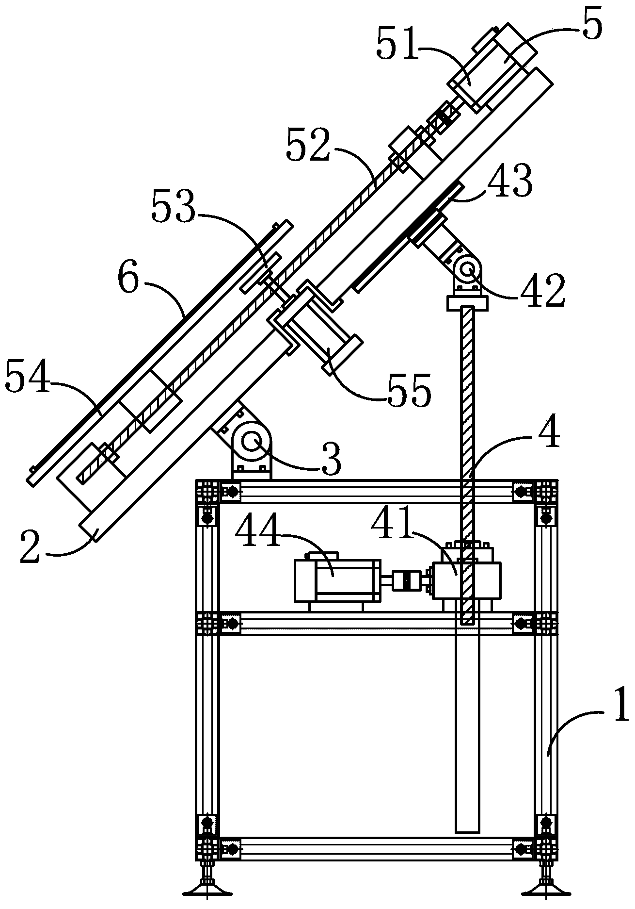
[0016] Such as figure 1 As shown, the OLED defect detection device of this embodiment includes a frame 1 , a mounting plate 2 , a posture adjustment assembly 4 , a detection adjustment assembly 5 , a clamping back plate 54 and a probe assembly 55 . The mounting bracket 2 is movably connected with the frame 1 through the fixed joint 3 , so that the mounting bracket 2 has a degree of freedom of rotation in a vertical plane relative to the frame 1 . The posture adjustment assembly 4 is connected between the frame 1 and the mounting pallet 2, and adjusts the inclination of the mounting pallet 2 by adjusting the rotation angle of the mounting pallet 2 in the vertical plane. The clamping backplane 54 is used to fix the OLED display screen, the clamping backplane 54 is connected with the detection and adjustment assembly 5, the detection and adjustme...


PUM


Abstract

The invention discloses a defect detection device for an OLED (Organic Light Emitting Diode), which comprises a rack, a mounting support plate, a gesture adjustment assembly, a detection adjustment assembly, a clamp mounting back plate and a probe assembly, wherein the mounting support plate is movably connected with the rack by a fixed joint, and provided with a rotational freedom degree of a vertical plane; the gesture adjustment assembly is connected between the rack and the mounting support plate, and used for adjusting inclination of the mounting support plate; the clamp mounting back plate is used for fixing an OLED display screen, and connected with the detection adjustment assembly; the detection adjustment assembly is fixedly mounted on the mounting support plate, and used for changing a relative position of the clamp mounting back plate and the mounting support plate; and the probe assembly is used for supplying power to the OLED display screen. The detection device has the benefits that when operating personnel control rotation of a motor, an inclination angle between an OLED panel and a horizontal plane can be adjusted according to personal height and operation habits; a fatigue degree of a worker on a mass production line can be relieved effectively; the working efficiency can be improved; and the detection quality can be ensured effectively.

Description

technical field [0001] The invention belongs to the field of organic light-emitting diode (OLED) display technology, relates to the back-end detection process of OLED mass production, and in particular to a defect detection device used in OLED mass production. Background technique [0002] Organic electroluminescent diode (OLED) display is called "dream display", which has the characteristics of all solid state, active light emission, high brightness, high contrast ratio, ultra-thin and ultra-light, low power consumption, no viewing angle limitation and wide operating temperature range. , is considered to be the next-generation flat-panel display emerging application technology. However, part of the structure of OLED displays, especially the electrodes and organic materials located therein, are extremely sensitive to external environmental factors such as oxygen and moisture. In actual use, the device needs to be packaged to isolate the device from water vapor and oxygen to ...

Claims


Application Information

Patent Timeline
IPC IPC(8): G01R31/26
Inventor 向欣任海朴章镐张晓茗王小月
Owner SICHUAN CCO DISPLAY TECH
Why Eureka
Try Eureka