Unlock instant, AI-driven research and patent intelligence for your innovation.

Memory erasing method and its driving circuit

A drive circuit and memory technology, applied in information storage, static memory, read-only memory, etc., can solve the problems of complex character line drive circuits and increase the occupied area, so as to simplify the circuit complexity and reduce the area occupied by the circuit Effect

Active Publication Date: 2016-07-20
EON SILICON SOLUTION
View PDF4 Cites 0 Cited by
  • Summary
  • Abstract
  • Description
  • Claims
  • Application Information

AI Technical Summary

Problems solved by technology

Too many suppression voltage circuits plus the division of storage segments will make the word line drive circuit too complicated. If you want to expand more storage blocks or storage stacks, you must repeatedly configure the drive circuit of the traditional NOR flash memory, so That will increase the occupied area

Method used


Image

  • Memory erasing method and its driving circuit
  • Memory erasing method and its driving circuit
  • Memory erasing method and its driving circuit

Examples


Embodiment Construction

[0049] In order to fully understand the purpose, characteristics and effects of the present invention, the present invention will be described in detail through the following specific embodiments, and in conjunction with the accompanying drawings, as follows:

[0050] In order to expand multiple rows and multiple columns of the NOR flash memory more easily to increase the capacity of the NOR flash memory without excessively increasing the chip size, the present invention provides a method for erasing memory and implementing the memory method By using the driving circuit of the present invention, multiple rows and multiple columns of the NOR flash memory can be increased without greatly increasing the chip size.

[0051] First, please refer to image 3 , image 3 It is a flow chart of the memory erasing method provided by the embodiment of the present invention. The NOR flash memory has multiple storage piles, each storage pile has multiple storage blocks, each storage block ...


PUM


Abstract

The present invention provides a memory erasing method and its driving circuit. The main technical solution includes: when the memory cells are selected to be erased, the gates of the multiple memory cells to be erased in the selected memory block, The drains of all memory cells in the selected memory stack and the gates of the unselected memory cells are set to float; provide positive voltage to all the sources of the selected memory stack and their shared P N-type well and N-type well; providing negative voltage to gates of multiple memory cells selected to be erased in the memory block. In this way, the floating gate can receive the coupling voltage from the positive electrode of the P-type well, and the erasure suppression of the unselected memory blocks can be achieved, making the decoding more simplified and easy to use with a smaller layout area Expansion to more memory blocks or memory heaps and partitioning of memory segments within memory blocks is achieved.

Description

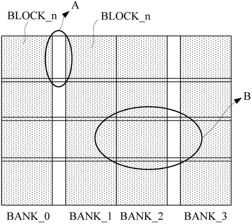
technical field [0001] The present invention relates to a NOR flash memory (NORFLASH MEMORY), and in particular to a memory erasing method suitable for a NOR flash memory, and a driving circuit for implementing the memory erasing method. Background technique [0002] With the progress of semiconductor technology, the capacity of memory is getting bigger and bigger, and its speed is getting faster and faster. Or non-type flash memory is currently widely used in electronic products, or non-type memory will have multiple storage banks (BANK), and each storage bank has multiple storage blocks (BLOCK), each storage bank It has multiple memory cells arranged in rows and columns. Generally speaking, multiple storage units in each storage block can share a P-type well (PWELL) and an N-type well (NWELL). When erasing multiple memory cells on a certain column in a certain memory block, traditionally, an erasing voltage (generally a relatively large positive voltage, such as 8V) will...

Claims


Application Information

Patent Timeline
Patent Type & Authority Patents(China)
IPC IPC(8): G11C16/14
Inventor 卢孝华郭志明王宇淳
Owner EON SILICON SOLUTION