Method for Monitoring Defect Detection Rate of Electron Beam Scanner

A technology of electron beam scanner and defect detection rate, which is applied in the direction of circuit, electrical components, semiconductor/solid-state device testing/measurement, etc., can solve problems such as damage and unreliable monitoring methods, and achieve promotion and avoid defect detection Inaccurate rate and accurate monitoring method

Active Publication Date: 2016-01-27
SHANGHAI HUALI MICROELECTRONICS CORP
View PDF5 Cites 0 Cited by
  • Summary
  • Abstract
  • Description
  • Claims
  • Application Information

AI Technical Summary

Problems solved by technology

The problem with this method is that since the E-beam is scanned by electron beams, it has a certain degree of destructive effect on the scanned area, so that the gray level of the long-term scanned area on the standard wafer will be significantly lower than other areas, so Repeatedly using the same standard wafer to test the defect detection rate of the E-beam machine is an obviously unreliable monitoring method

Method used


Image

  • Method for Monitoring Defect Detection Rate of Electron Beam Scanner
  • Method for Monitoring Defect Detection Rate of Electron Beam Scanner
  • Method for Monitoring Defect Detection Rate of Electron Beam Scanner

Examples


Embodiment Construction

[0014] The specific embodiment of the present invention will be further described in detail below in conjunction with the accompanying drawings.

[0015] Such as figure 1 As shown, the method for monitoring the defect detection rate of an electron beam scanner provided by an embodiment of the present invention includes the following steps:

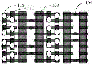
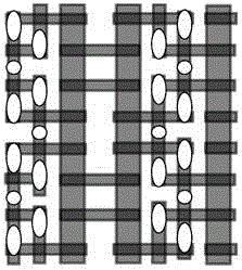
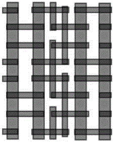
[0016] Step S10 , establishing three test units in the first area of ​​the CMOS wafer, which are respectively the first, second and third test units, and each test unit includes an NMOS area and a PMOS area.

[0017] Wherein, the first region can be any region on the wafer, and its size is the same as that of a chip unit; in a preferred embodiment, the first region is located on the dicing lane of the wafer. Establishing test units on the dicing lanes of the wafer does not occupy the position of valid chip units on the wafer and causes no waste. In the subsequent process, when the wafer is diced, the test unit is destroyed.

[0018] The...


PUM


Abstract

The invention relates to a method for monitoring a defect detection rate of an electron beam scanner. The method comprises the following steps that three test units are built in the first region of a CMOS wafer; a plurality of first connecting holes are vertically formed in the first test unit and are filled with metal, a plurality of second connecting holes are vertically formed in the second test unit and are filled with metal, and a plurality of third connecting holes are vertically formed in the third test unit and are filled with metal; the bottom ends of the first connecting holes are connected with a PMOS region, the bottom ends of the second connecting holes are connected with the active region of an NMOS region, and the bottom ends of the third connecting holes are connected with the gate region of the NMOS region; the first test unit, the second test unit and the third test unit are respectively scanned through the electron beam scanner, the first connecting holes, the second connecting holes and the third connecting holes are detected through the comparison of the standard gray levels of the first connecting holes, the second connecting holes and the third connecting holes respectively, and the detection rate of the first connecting holes, the detection rate of the second connecting holes and the detection rate of the third connecting holes are recorded; the CMOS wafer is replaced with a next CMOS wafer, and the above steps are repeated. The monitor method is more accurate, more reliable and beneficial for being promoted in the field of semiconductor industries.

Description

technical field [0001] The invention relates to the field of semiconductor processing and manufacturing, and more specifically relates to a method for monitoring the defect detection rate of an electron beam scanner. Background technique [0002] With the development of integrated circuit technology and the scaling down of key dimensions, as well as the increase in the complexity of semiconductor manufacturing, electron beam scanners (E-beam) are increasingly used in semiconductor production, such as 55nm and below technology Insufficient etching defects of tungsten connection holes and copper connection holes of nodes, as well as dislocation leakage defects and nickel pipeline leakage defects all need to be detected by E-beam, and they are irreplaceable in the current process. In order to ensure the accuracy of the data of the electron beam defect scanner and prevent the performance change of E-beam itself from adversely affecting the process; therefore, it is necessary to ...

Claims


Application Information

Patent Timeline
Patent Type & Authority Patents(China)
IPC IPC(8): H01L21/66
CPCH01L22/12H01L22/20H01L22/30
Inventor 范荣伟龙吟倪棋梁陈宏璘
Owner SHANGHAI HUALI MICROELECTRONICS CORP
Why Eureka
Try Eureka