Mass production testing method of CIS chip

A test method and chip technology, applied in electronic circuit testing and other directions, can solve the problems of rising chip testing costs, high testing machine prices, and reduced test program execution efficiency, and achieve the effect of improving computing speed and shortening data processing time.

Active Publication Date: 2014-02-05
豪威半导体(太仓)有限公司
View PDF8 Cites 49 Cited by
  • Summary
  • Abstract
  • Description
  • Claims
  • Application Information

AI Technical Summary

Problems solved by technology

[0007] As a result, the price of the test machine is very high; moreover, since all data must be uploaded to the workstation for unified processing, in the multi-station chip parallel test mode, all data processing can only be performed serially, which seriously reduces the test performance. The execution efficiency of the program will lead to a substantial increase in the cost of chip testing and affect the competitiveness of the product

Method used


Image

  • Mass production testing method of CIS chip
  • Mass production testing method of CIS chip

Examples


Embodiment Construction

[0040] In order to make the object, technical solution and advantages of the present invention clearer, the present invention will be further described in detail below in conjunction with the embodiments and accompanying drawings. It should be understood that the specific embodiments described here are only used to explain the present invention, not to limit the present invention.

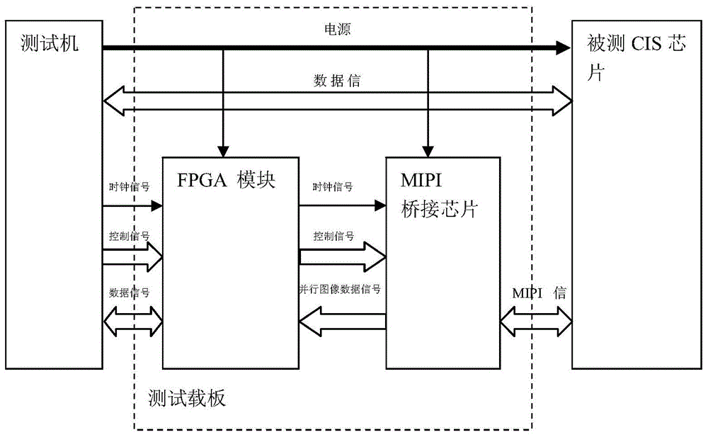
[0041] The present invention relates to the mass production test technology of CIS (CMOS Image Sensor) chip with MIPI (Mobile Industry Processor Interface) high-speed port of the mobile communication industry processor interface. The technology can adopt Field Programmable Gate Array FPGA (Field Programmable Gate Array) chip and MIPI serial-to-parallel data bridge chip to realize the CP (Chip Probe) test and FT (Final Test) test for mass production of CIS chips.

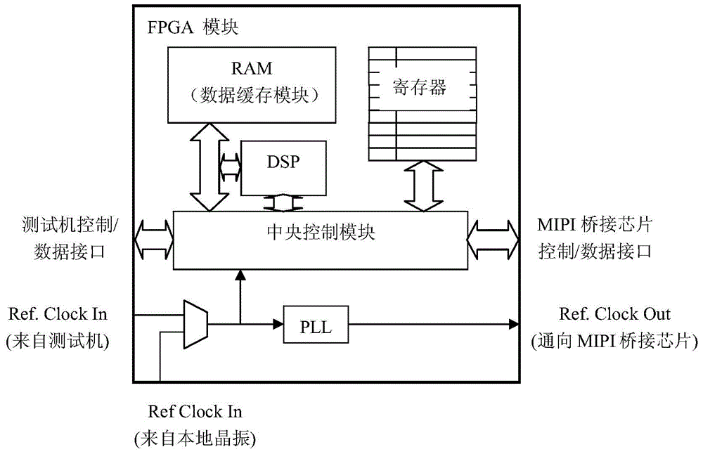
[0042] figure 1 Shown is the CIS chip test system based on the FPAG module (FPAG chip) used in an embodiment of the present invention, ...


PUM


Abstract

The invention discloses a mass production testing method of a CIS chip. The method is carried out based on an FPGA module and includes the steps that a testing system provided with a testing machine and a testing carrier plate is provided, wherein an MIPI bridge chip and the FPGA module are installed on the testing carrier plate; the CIS chip is controlled by the testing machine to collect an image; image data are output to the MIPI bridge chip by the CIS chip in a high-speed serial signal mode; the MIPI bridge chip is controlled by the FPGA module to read high-speed serial signals, convert the high-speed serial signals to parallel low-speed data signals and upload the parallel low-speed data signals to the FPGA module; the parallel low-speed data signals are read by the FPGA module, technical processing is carried out, and calculation results are acquired and are uploaded under the control of the testing machine; judgment and program flow control are carried out after the results are read by the testing machine. Data conversion carried out through the specific MIPI bridge chip avoids dependence on high-speed signal ports of the testing machine; due to the adoption of DSP data processing in the FPGA module, the data calculation speed is improved, and multi-station parallel data calculation is achieved and shortens data processing time when compared with serial calculation on a testing machine working station.

Description

technical field [0001] The invention relates to the technical field of mass production testing of integrated circuits, in particular to an FPGA-based mass production testing method for CIS chips with MIPI ports. Background technique [0002] The existing high-end CIS (CMOS Image Sensor) chip has reached a resolution of more than 5 million pixels, that is to say, each frame of image data sampled by it will contain at least 500 sets of image data; and in order to improve data transmission efficiency Most of the chips use the Mobile Industry Processor Interface (MIPI) as the channel for image data transmission, and the data output rate can reach up to 1Gbps. [0003] The traditional CIS chip mass production test method is generally processed by professional high-end ATE automatic test equipment (Automatic Test Equipment). To meet the test requirements of high-end CIS chips, these ATE devices must meet the following conditions: [0004] (1) A high-speed workstation is used to ...

Claims


Application Information

Patent Timeline
Patent Type & Authority Applications(China)
IPC IPC(8): G01R31/28
Inventor 关牮
Owner 豪威半导体(太仓)有限公司
Why Eureka
Try Eureka