LED epitaxy structure

A technology of epitaxial structure and structural layer, which is applied in the direction of electrical components, circuits, semiconductor devices, etc., can solve problems such as LED failure, PN junction breakdown, and small distance between them, so as to achieve reduced failure rate, extended service life, and high reliability. high effect

Active Publication Date: 2014-02-05
EPITOP PHOTOELECTRIC TECH
View PDF4 Cites 3 Cited by
  • Summary
  • Abstract
  • Description
  • Claims
  • Application Information

AI Technical Summary

Problems solved by technology

[0003] The two positive and negative electrodes of traditional LEDs are on the same surface of the chip, and the distance between them is small. Through electrostatic discharge ESD, electrostatic charges are easy to accumulate at both ends of the LED and then genera

Method used


Image

  • LED epitaxy structure
  • LED epitaxy structure
  • LED epitaxy structure

Examples


Embodiment 1

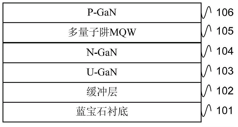
[0015] 1. Put the patterned (Patterned Sapphire Substrate, PSS) sapphire substrate (which can be other material substrates such as GaN) 201 into the reaction chamber, N 2 :H 2 : NH 3 The flow ratio is (0:120:0) SLM, the pressure in the reaction chamber is 500 Torr, the temperature is raised to 1080 °C, the rotation speed is 1200 (rev / s), and the stability is 300 s, and the substrate is purified at high temperature.

[0016] 2. Lower the temperature to 540°C, the ratio of N2:H2:NH3 is (75:150:56) SLM, the pressure of the reaction chamber is controlled at 500 Torr, the rotation speed is 600 (rev / sec), and a 35nm-thick low-temperature GaN buffer layer 202 is grown.

[0017] 3. Raise the temperature to 1080 °C, the ratio of N2:H2:NH3 is (75:150:56) SLM, the pressure of the reaction chamber is controlled at 200 Torr, the rotation speed is 1200 (rev / sec), and the high temperature undoped 1000 nm thick is grown. GaN layer (U-GaN) 203 .

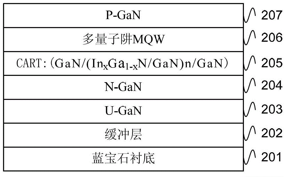
[0018] 4. Keep the temperature at 1050°C, t...


PUM

PropertyMeasurementUnit
Thicknessaaaaaaaaaa

Abstract

The invention provides an LED epitaxy structure. The LED epitaxy structure comprises a substrate. A buffer layer is arranged on the substrate. The surface of the buffer layer is provided with an undoped GaN layer. The surface of the undoped GaN layer is provided with an N-type doped GaN layer. The surface of the N-type doped GaN layer is provided with an asymmetric resonant tunnel CART structure layer. The surface of the CART structure layer is provided with a multiple quantum well MQW layer. A P-type doped GaN layer is arranged on the MQW layer. According to the embodiments of the invention, the LED electrostatic discharge (Electro-Static Discharge, ESD) resistance capability can be effectively improved.

Description

technical field [0001] The invention relates to the field of semiconductor devices, in particular to an LED epitaxial structure. Background technique [0002] The traditional structure of GaN-based LED structure such as figure 1 As shown, including: sapphire substrate 101, buffer layer 102, undoped GaN layer (U-GaN) 103, N-type doped GaN layer (N-GaN) 104, multiple quantum well MQW layer 105 and P-type Doped GaN layer (P-GaN) 106 . [0003] The two positive and negative electrodes of traditional LEDs are on the same side of the chip, and the distance between them is small. Through electrostatic discharge ESD, electrostatic charges are easily accumulated at both ends of the LED, thereby generating electrostatic voltage. When the electrostatic voltage increases to a certain value, It will cause the PN junction to break down and increase its leakage. In severe cases, the PN junction will also break down to a short circuit, causing the LED to fail. SUMMARY OF THE INVENTION ...

Claims


Application Information

Patent Timeline
IPC IPC(8): H01L33/06
CPCH01L33/06H01L33/32
Inventor 焦建军黄小辉李晓莹周德保郑远志陈向东康建梁旭东
Owner EPITOP PHOTOELECTRIC TECH
Why Eureka
Try Eureka