Layout design method of novel ESD diode
A layout design and diode technology, which is applied in the layout design field of new ESD diodes, can solve problems such as failure to reach ESD, ESD diode damage, etc., and achieve the effect of improving anti-ESD ability and excellent anti-ESD performance
- Summary
- Abstract
- Description
- Claims
- Application Information
AI Technical Summary
Problems solved by technology
Method used
Image
Examples
Embodiment Construction
[0020] The present invention will be further described below in conjunction with the accompanying drawings and specific embodiments.
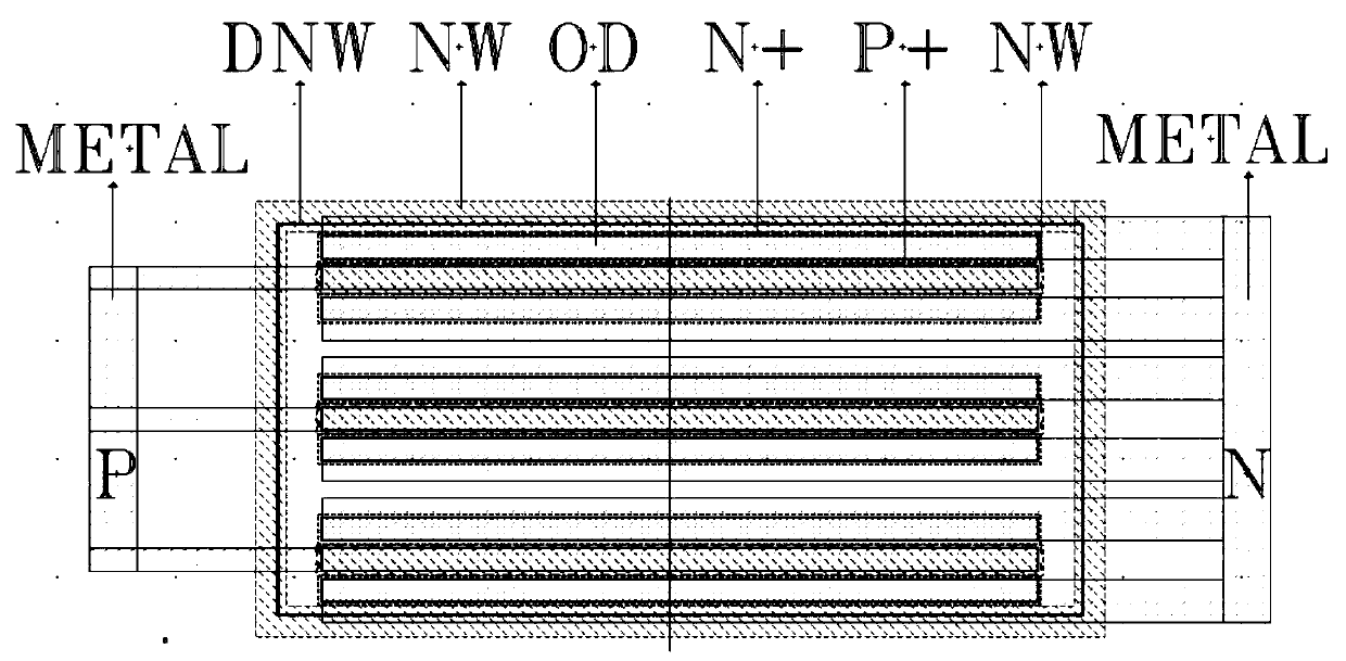
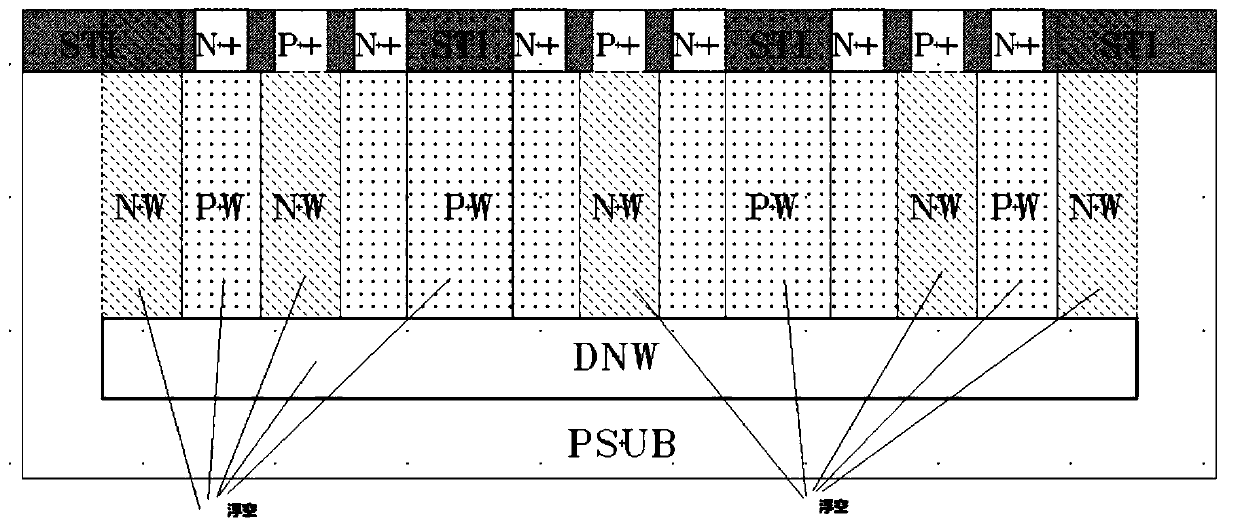
[0021] Such as Figure 1-4 As shown, the present invention provides a kind of layout design method of novel ESD diode, comprises the following steps:
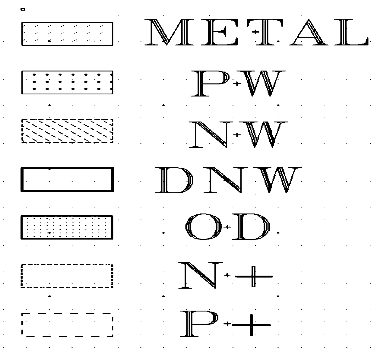
[0022] First of all, the English abbreviations used in the present invention are: METAL (metal wiring), PW (P well), NW (N well), DNW (deep N well), OD (active diffusion region), N+ (N Type implantation region), P+ (P-type implantation region), STI (shallow trench isolation region), CMOS (complementary metal oxide semiconductor), PSUB (P-type substrate), CONTACT (contact hole).
[0023] The technology that ESD diode of the present invention needs is CMOS technology (with DNW), designs a DNW on the P-type substrate, designs a NW ring and connects with DNW around DNW, forms a large DNW enclosed area now; Then design NW and PW in the DNW closed area, design a PW on both sides of the NW (the NW an...
PUM
 Abstract
Description
Claims
Application Information


