PLDMOS for ESD protection
An ESD protection and epitaxial layer technology, applied in electrical components, circuits, semiconductor devices, etc., can solve the problems of reduced ESD resistance and high ESD current density of PLDMOS, avoiding ESD current concentration and improving ESD resistance. Effect
- Summary
- Abstract
- Description
- Claims
- Application Information
AI Technical Summary
Problems solved by technology
Method used
Image
Examples
Embodiment Construction
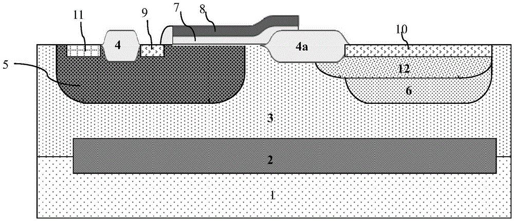
[0039] Such as figure 2 As shown, it is a schematic structural diagram of the PLDMOS used for ESD protection in the embodiment of the present invention; the PLDMOS used in the ESD protection in the embodiment of the present invention includes:
[0040] P-type epitaxial layer 3 . The P-type epitaxial layer 3 is formed on the surface of a semiconductor substrate such as a silicon substrate 1 , and an N-type buried layer 2 is formed at the bottom of the P-type epitaxial layer 3 .
[0041] The channel region 5 is composed of an N well formed in the P-type epitaxial layer 3 .
[0042] A drift region, the composition of the drift region includes a P well 6 formed in the P-type epitaxial layer 3; there is a lateral distance between the P well 6 and the channel region 5, and the P well 6 and the surface of the P-type epitaxial layer 3 between the channel region 5 is formed with a first local field oxide layer 4a, the first side edge of the first local field oxide layer 4a and the p...
PUM
 Abstract
Description
Claims
Application Information


