Semiconductor structure and fin field-effect tube forming method and etching device

A technology of a fin field effect transistor and an etching device, which is applied to the device for coating liquid on the surface, the manufacture of semiconductor devices, and semiconductor/solid state devices, etc. , the depth of the second groove 18 is difficult to control, etc., to achieve the effect of improving accuracy, high precision and improving performance

Active Publication Date: 2014-02-12
SEMICON MFG INT (SHANGHAI) CORP
View PDF5 Cites 4 Cited by
  • Summary
  • Abstract
  • Description
  • Claims
  • Application Information

AI Technical Summary

Problems solved by technology

[0009] Currently, when the isolation structure 11 is etched back to form the second groove 18, the depth of the second groove 18 is difficult to control, so that the width of the surface of the exposed fin 14 (the width of the upper surface and the exposed two sides The sum of the heights of the side walls) is prone to change, and the change in the width of the surface of the exposed fin 14 will cause the threshold voltage of the FinFET to shift after the gate structure is formed, affecting the finFET stability

Method used


Image

  • Semiconductor structure and fin field-effect tube forming method and etching device
  • Semiconductor structure and fin field-effect tube forming method and etching device
  • Semiconductor structure and fin field-effect tube forming method and etching device

Examples


Embodiment Construction

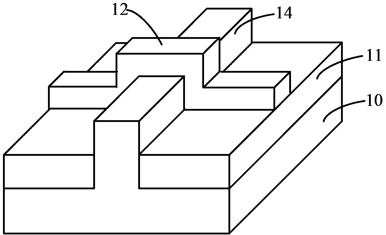
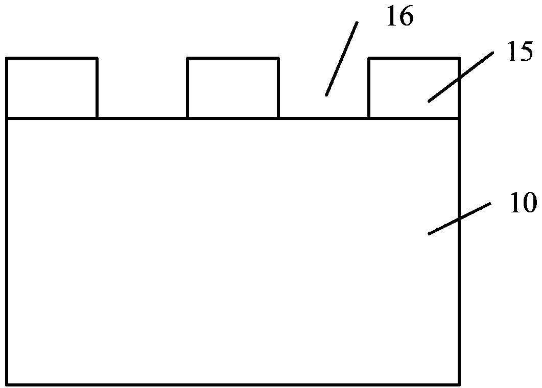
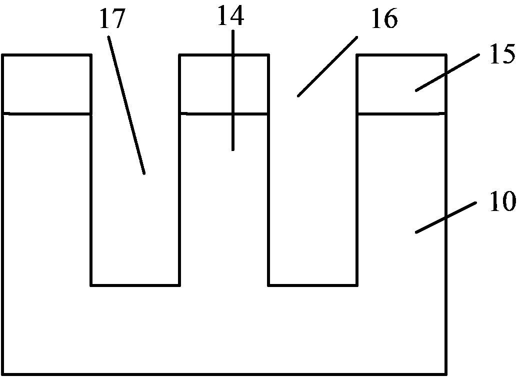
[0052] In the production process of the existing fin field effect transistor, the process of etching back the height of the exposed part of the isolation structure is a dry etching process or a wet etching process, but it is difficult to control the end point of the etching by using the existing etching process , so that it is difficult to accurately control the depth of the isolation structure being etched back, so that there is an error in the width of the exposed fin surface, and after the gate structure is formed on the exposed fin surface, the threshold voltage of the FinFET will be biased. Shift, affecting the stability of the FinFET.

[0053] In order to solve the above problems, the inventor proposes an etching device and a method for forming a semiconductor structure and a fin field effect transistor by using the etching device. In the method for forming the fin field effect transistor, when etching back the isolation structure, first A process of spraying liquid is c...


PUM


Abstract

The invention discloses a semiconductor structure and fin field-effect tube forming method and an etching device. The fin field-effect tube forming method comprises the step of providing a semiconductor substrate; the step of etching the semiconductor substrate to form a plurality of fin parts, wherein first grooves are formed between every two adjacent fin parts; the step of filling the first grooves with isolation materials to form an isolation structure; the step of spraying liquid, spraying a layer of liquid on the surface of the isolation structure and the surfaces of the fin parts, wherein the semiconductor substrate is rotated in the process of spraying; the step of supplying reaction gas, wherein the reaction gas is blended with the layer of liquid spraying the surface of the isolation structure and the surfaces of the fin parts to form an etching solution used for etching the isolation structure; the step of executing the liquid spraying process and the reaction gas supplying process repeatedly until the isolation structure is removed by certain thickness to form a second groove and to expose the fin parts by certain height; the step of forming a gate structure striding the surfaces and the side walls of the fin parts which are exposed by the certain height. The precision of removing the isolation structure by the certain thickness is improved.

Description

technical field [0001] The invention relates to the field of semiconductor manufacturing, in particular to a method for forming a semiconductor structure and a fin field effect transistor, and an etching device. Background technique [0002] With the continuous development of semiconductor process technology, as the process node gradually decreases, gate-last (gate-last) process has been widely used to obtain an ideal threshold voltage and improve device performance. However, when the feature size (CD, Critical Dimension) of the device is further reduced, even if the gate-last process is adopted, the structure of the conventional MOS field effect transistor can no longer meet the requirements for device performance. Fin field effect transistor (Fin FET) as Substitution of conventional devices has received extensive attention. [0003] figure 1 A schematic diagram of a three-dimensional structure of a fin field effect transistor in the prior art is shown. like figure 1 As...

Claims


Application Information

Patent Timeline
Patent Type & Authority Applications(China)
IPC IPC(8): H01L21/306H01L21/28H01L21/336B05C5/02
CPCH01L21/31111H01L29/0649H01L29/66621H01L29/66795
Inventor 三重野文健
Owner SEMICON MFG INT (SHANGHAI) CORP
Why Eureka
Try Eureka