Check patentability & draft patents in minutes with Patsnap Eureka AI!

Defect density calculation method

A technology of defect density and calculation method, which is applied in the direction of electrical components, circuits, semiconductor/solid-state device testing/measurement, etc., can solve the problems of defect density error, unconsidered device test item coefficient, etc., and achieve the effect of reducing error

Active Publication Date: 2016-06-15
CSMC TECH FAB2 CO LTD
View PDF3 Cites 0 Cited by
  • Summary
  • Abstract
  • Description
  • Claims
  • Application Information

AI Technical Summary

Problems solved by technology

[0011] In the above model calculation formula, N represents the complexity coefficient. In the existing algorithm, only the number of photolithography layers is used to calculate the value of the complexity coefficient N, but it does not take into account the different device test item coefficients and different process technologies. Density 0 caused by the influence, so the calculated defect density D 0 there is a big error

Method used


Image

  • Defect density calculation method
  • Defect density calculation method
  • Defect density calculation method

Examples


Embodiment Construction

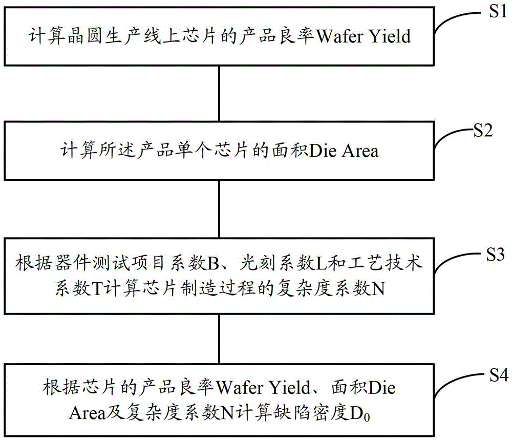
[0041] The invention discloses a defect density calculation method, comprising the following steps:

[0042] S1. Calculate the product yield WaferYield of the chip on the wafer production line;

[0043] S2. Calculate the area DieArea of ​​a single chip of the product;

[0044] S3. Calculate the complexity coefficient N of the chip manufacturing process of the product according to the device test item coefficient DeviceTestBin, the lithography coefficient LithoCoefficient and the process technology coefficient TechnologyCoefficient;

[0045] S4. Calculate the defect density D according to the product yield rate WaferYield of the chip, the area DieArea and the complexity coefficient N 0 .

[0046] The present invention calculates the complexity coefficient N through the device test item coefficient B, the lithography coefficient L and the process technology coefficient T, and calculates the defect density through the corrected N, which reduces the error between the defect dens...


PUM


Abstract

The invention discloses a defect density calculating method. The defect density calculating method comprises the steps that S1, the wafer yield of chips on a wafer production line is calculated; S2, the die area of a single chip of products is calculated; S3, the complexity coefficient N of the products in a chip manufacturing process is calculated according to the device test bin coefficient, the litho coefficient and the technology coefficient; S4, the defect density D0 is calculated according to the wafer yield, the die area and the complexity coefficient N of the chips. According to the defect density calculating method, the complexity coefficient N is calculated according to the device test bin coefficient B, the litho coefficient L and the technology coefficient T, the defect density is calculated through the modified N, and the deviation of the defect density and actual wafer processing ability is reduced. Meanwhile, the calculating method and the technological process will not produce additional cost.

Description

technical field [0001] The invention relates to the technical field of semiconductors, in particular to a defect density calculation method. Background technique [0002] At present, the semiconductor manufacturing process is to grow hundreds of thousands of identical chips on a wafer at the same time, and the wafer after all the processes are completed is also called a bare chip. Qualified chips are selected by testing the bare chips, and cut and packaged into products. Usually, the calculation method of WaferYield for a certain product yield rate of a wafer production line is to first randomly select a number of dies of this product produced by the same wafer production line (the number can vary according to the production situation), and then test all the selected dies. For all chips on the bare chip, use the calculation formula of WaferYield: [0003] WaferYield=Number of qualified chips / total number of chips [0004] Get the product yield WaferYield of a certain prod...

Claims


Application Information

Patent Timeline
Patent Type & Authority Patents(China)
IPC IPC(8): H01L21/66
CPCH01L22/10H01L22/20
Inventor 陈亚威
Owner CSMC TECH FAB2 CO LTD
Features
  • R&D
  • Intellectual Property
  • Life Sciences
  • Materials
  • Tech Scout
  • Unparalleled Data Quality
  • Higher Quality Content
  • 60% Fewer Hallucinations
Learn More