Static Random Access Memory and Write Redundancy Improvement Method in Embedded SiGe Process

An embedded germanium-silicon, static random technology, used in semiconductor/solid-state device manufacturing, electrical solid-state devices, semiconductor devices, etc., can solve the problems of small equivalent resistance and low write redundancy, and achieve increased equivalent Resistance, improved hole mobility, reduced compressive stress

Active Publication Date: 2016-08-17
SHANGHAI HUALI MICROELECTRONICS CORP
View PDF6 Cites 0 Cited by
  • Summary
  • Abstract
  • Description
  • Claims
  • Application Information

AI Technical Summary

Problems solved by technology

However, in the SRAM in the existing embedded silicon germanium process, the equivalent resistance of the pull-up transistor is small, which in turn leads to a small write margin (Write Margin) of the SRAM

Method used


Image

  • Static Random Access Memory and Write Redundancy Improvement Method in Embedded SiGe Process
  • Static Random Access Memory and Write Redundancy Improvement Method in Embedded SiGe Process
  • Static Random Access Memory and Write Redundancy Improvement Method in Embedded SiGe Process

Examples


Embodiment Construction

[0021] In order to illustrate the technical content, structural features, achieved goals and effects of the present invention in detail, the following will be described in detail in conjunction with the embodiments and accompanying drawings.

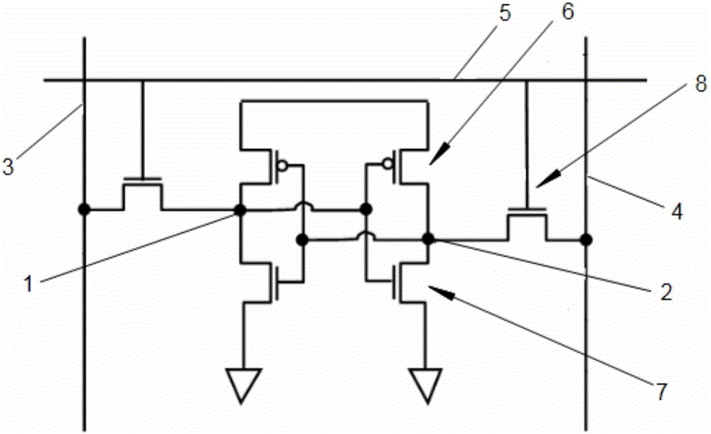
[0022] see figure 1 , figure 1 Shown is a schematic diagram of an equivalent circuit for writing SRAM in the embedded silicon germanium process of the present invention. Write margin (Write Margin) is an important parameter to measure the writing performance of SRAM cells in the embedded SiGe process. In the equivalent circuit for writing SRAM in the embedded silicon germanium process, it is assumed that the first node 1 stores data at a low potential (that is, the stored data is "0"), and the second node 2 stores data It is a high potential (that is, the stored data is "1"), non-limiting enumeration, for example, writing a high potential to the first node 1, writing a low potential to the second node 2, before the writing action, The...


PUM


Abstract

A static random access memory in an embedded silicon germanium process, comprising: a silicon-based substrate; an NMOS device; a PMOS device, the gate of the PMOS device is arranged on the silicon-based substrate, and the source region and the drain region of the PMOS device are respectively arranged In the silicon-based substrate on both sides of the gate, embedded silicon germanium is arranged in the source region and the drain region; the pull-up transistor is a PMOS semiconductor, and the gate of the pull-up transistor is arranged on the silicon-based substrate. The source region and the drain region of the pull-up transistor are respectively arranged in the silicon base substrate on both sides of the gate. The present invention increases the compressive stress in the channel of the PMOS device by arranging embedded silicon germanium in the source region and the drain region of the PMOS device, thereby improving the hole mobility; There is no embedded silicon germanium in the drain region, so that the compressive stress of the pull-up transistor in the channel direction is reduced, the carrier mobility is reduced, and the equivalent resistance of the pull-up transistor is increased, thereby improving the static randomness. Memory write redundancy.

Description

technical field [0001] The invention relates to the technical field of semiconductors, in particular to a static random access memory in an embedded silicon germanium process and a method for improving write redundancy. Background technique [0002] As an important product in semiconductor memory, Static Random Access Memory (SRAM) in the embedded silicon germanium process has been widely used in high-speed data exchange systems such as computers, communications, and multimedia. [0003] Generally, the layout of the SRAM in the embedded silicon germanium process below 90nm includes three levels of active regions, polysilicon gates, and contact holes, and control transistors are respectively formed on the layout areas, and the control transistors is an NMOS device; a pull down transistor (Pull Down MOS), the pull down transistor is an NMOS device; a pull up transistor (Pull Up MOS), the pull up transistor is a PMOS device. However, in the SRAM in the existing embedded silico...

Claims


Application Information

Patent Timeline
Patent Type & Authority Patents(China)
IPC IPC(8): H01L27/11H01L29/08H01L21/8244
Inventor 俞柳江
Owner SHANGHAI HUALI MICROELECTRONICS CORP
Why Eureka
Try Eureka