Manufacturing method for PMOS transistor and manufacturing method for NMOS transistor

A manufacturing method and transistor technology, applied in the direction of transistors, semiconductor/solid-state device manufacturing, semiconductor devices, etc., can solve problems such as slow carrier mobility, improve process compatibility, improve migration rate, increase compressive stress or tension The effect of stress

Active Publication Date: 2014-10-15
SEMICON MFG INT (SHANGHAI) CORP
View PDF6 Cites 20 Cited by
  • Summary
  • Abstract
  • Description
  • Claims
  • Application Information

AI Technical Summary

Problems solved by technology

[0007] The technical problem to be solved by the present invention is to improve the problem that the carrier transfer rate of PMOS transistor and NMOS transistor is too slow

Method used


Image

  • Manufacturing method for PMOS transistor and manufacturing method for NMOS transistor
  • Manufacturing method for PMOS transistor and manufacturing method for NMOS transistor
  • Manufacturing method for PMOS transistor and manufacturing method for NMOS transistor

Examples


Embodiment 1

[0047] In this embodiment, two stacked stepped sigma-shaped grooves are taken as an example to describe the manufacturing method of the PMOS transistor in detail.

[0048] Figure 1 to Figure 8 is a cross-sectional view of a PMOS transistor at different fabrication stages in an embodiment of the present invention, which will be combined below Figure 1 to Figure 8 The production method will be described in detail.

[0049] Step S1 is first performed: provide a silicon substrate, and form a gate structure on the silicon substrate. The gate structure includes a gate dielectric layer formed on the silicon substrate and a gate electrode formed on the gate dielectric layer.

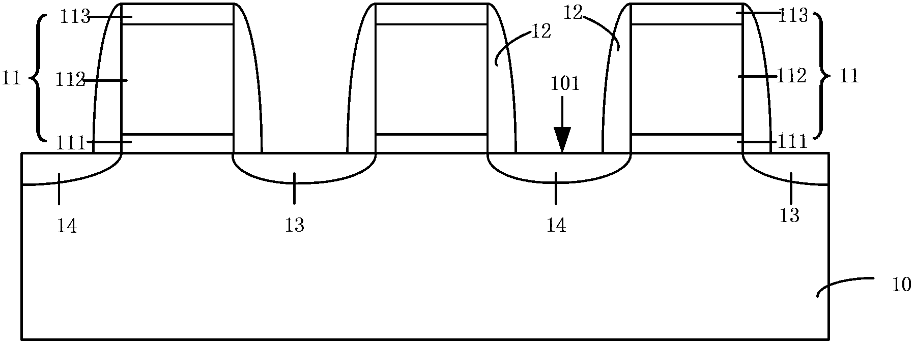
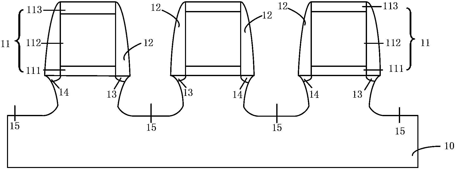
[0050] Such as figure 1 As shown, the substrate 10 is a single crystal silicon substrate having a surface 101 . A shallow trench isolation structure (Shallow Trench Isolation, STI for short) (not shown) may be formed in the substrate 10 to isolate active regions in the substrate 10 .

[0051] The gate struc...

Embodiment 2

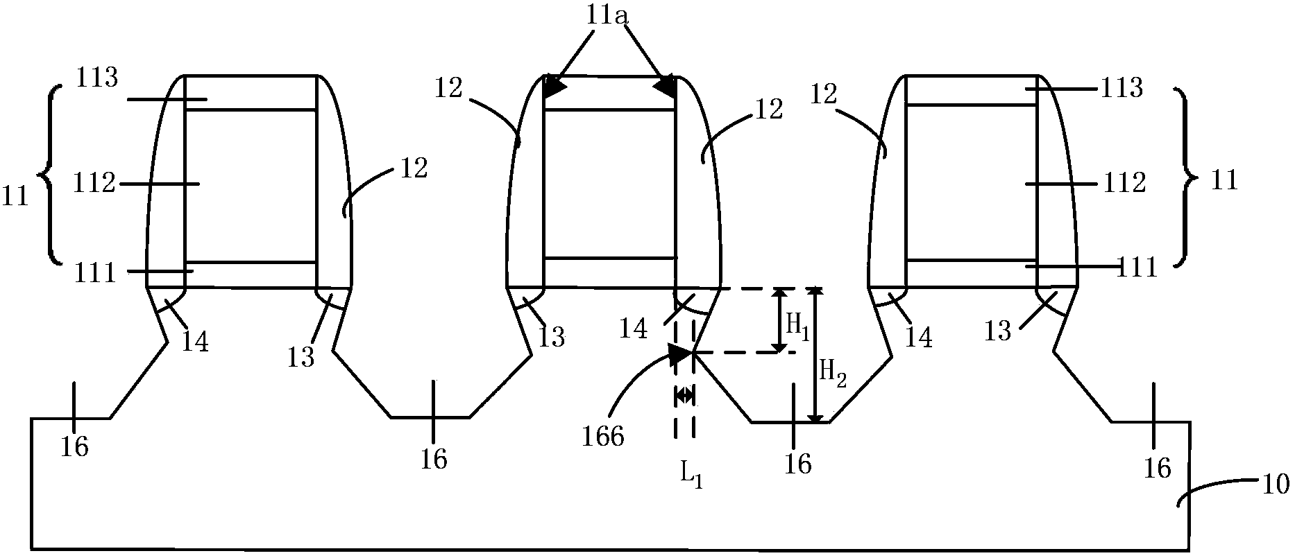
[0080] As described in Embodiment 1, a plurality of stacked sigma-shaped grooves deep into the silicon substrate are formed in the source and drain regions, and in the direction from the surface of the silicon substrate to the inside of the silicon substrate, each sigma-shaped groove The tip of the groove that goes deep into the channel tends to gradually move away from the channel. Filling such a plurality of stacked sigma-shaped grooves with silicon germanium material can increase the hole carrier mobility rate of the channel of the PMOS transistor.

[0081] Based on the above inventive concept, the second embodiment proposes to form a third sigma-shaped groove in the silicon substrate at the bottom of the second sigma-shaped groove, and form a fourth sigma-shaped groove in the silicon substrate at the bottom of the third sigma-shaped groove. Groove, ... and so on, forming a stepped sigma-shaped groove in which a plurality of sigma-shaped grooves are stacked, and the distance...

Embodiment 3

[0084] The third embodiment provides an NMOS transistor and its formation method, except that silicon carbide is filled in multiple stacked stepped sigma-shaped grooves to apply tensile stress to the channel, and the rest of the method and structure are the same as those of the first to first embodiments above. The two are the same, by making the direction from the surface of the silicon substrate to the inside of the silicon substrate, the groove tip of each sigma-shaped groove deep into the channel is a stepped sigma-shaped groove that gradually moves away from the channel to improve the silicon carbide The filling amount of material to increase the mobility of electron carriers in the channel.

[0085] The process of filling silicon carbide into multiple stacked stepped sigma-shaped grooves refers to the existing process.

[0086] In the present invention, each embodiment adopts a progressive writing method, focusing on the differences from the foregoing embodiments. For th...


PUM


Abstract

The invention provides a manufacturing method for a PMOS transistor and a manufacturing method for an NMOS transistor. According to the aforementioned manufacturing methods, multiple laminated sigma-shaped grooves (at least two), i.e. stepped sigma-shaped grooves, are formed in source electrode and drain electrode regions in a direction of being perpendicular to the surface of a silicon substrate. In the direction from the surface of the silicon substrate into the silicon substrate, the groove tip, which stretches into a channel, of each sigma-shaped groove presents to be away from the channel gradually. Then a) as for the PMOS transistor, silicon germanium material is filled in the stepped sigma-shaped grooves so that pressure stress is applied to the channel, b) and as for the NMOS transistor, silicon carbide material is filled in the stepped sigma-shaped grooves so that pulling stress is applied to the channel. Therefore, capacity of the stepped sigma-shaped grooves is larger, and more silicon germanium material or silicon carbide material can be accommodated. Correspondingly, pressure stress or pulling stress to the channel is increased so that migration rate of hole carriers or electron carriers is improved.

Description

technical field [0001] The invention belongs to the field of semiconductor manufacturing, and in particular relates to a manufacturing method of a PMOS transistor and a manufacturing method of an NMOS transistor. Background technique [0002] With the improvement of integrated circuit integration, the size of semiconductor devices is gradually scaled down. In the process of scaling down the size of semiconductor devices, the drain voltage does not decrease accordingly, which leads to the gap between the source and drain. The electric field in the track area increases, and under the action of a strong electric field, electrons will accelerate to a speed many times higher than the speed of thermal motion between two collisions. Because the kinetic energy of electrons is very large, the electrons are called hot electrons, which cause hot electrons Effect (hot electron effect). The hot electron effect will cause hot electrons to be injected into the gate dielectric layer, formi...

Claims


Application Information

Patent Timeline
Patent Type & Authority Applications(China)
IPC IPC(8): H01L21/336
CPCH01L29/0847H01L29/1608H01L29/161H01L29/66568
Inventor 李凤莲倪景华
Owner SEMICON MFG INT (SHANGHAI) CORP
Why Eureka
Try Eureka