Liquid crystal display panel and liquid crystal display device

A technology of liquid crystal display panel and liquid crystal display device, which is applied in static indicators, instruments, nonlinear optics, etc., can solve the problems of complex design of data driving circuit and high cost

Active Publication Date: 2014-02-19
SHANGHAI TIANMA MICRO ELECTRONICS CO LTD
View PDF2 Cites 11 Cited by
  • Summary
  • Abstract
  • Description
  • Claims
  • Application Information

AI Technical Summary

Problems solved by technology

[0006] Aiming at the zigzag typesetting structure of the display panel with column inversion to realize dot inversion mode in the prior art, which leads to the problem of complex design of data drive circuit and high cost, no effective solution has been proposed at present. For this reason, the main purpose of the present invention The purpose is to provide a liquid crystal display panel and a liquid crystal display device to solve the above problems

Method used


Image

  • Liquid crystal display panel and liquid crystal display device
  • Liquid crystal display panel and liquid crystal display device
  • Liquid crystal display panel and liquid crystal display device

Examples


Embodiment 1

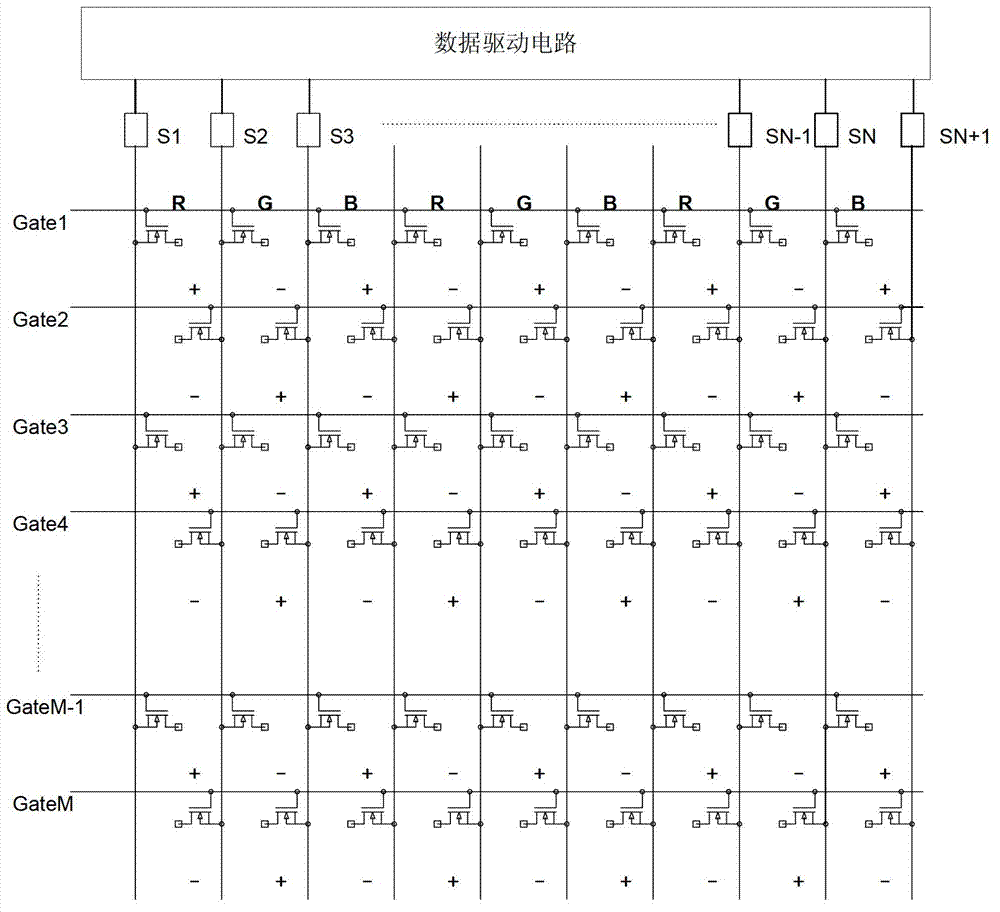
[0063] figure 2 is a schematic diagram of a circuit structure of a liquid crystal display panel according to Embodiment 1 of the present invention.

[0064] like figure 2 As shown, this embodiment provides a liquid crystal display panel, which includes:

[0065] A plurality of sub-pixels, the plurality of sub-pixels are arranged in a matrix of M rows×N columns;

[0066] N+1 parallel data lines S1, S2, ... , SN, SN+1, each data line is used to receive and transmit pixel data;

[0067] And M scanning lines Gate1, Gate2, . . . , GateM-1, GateM perpendicularly intersecting each data line.

[0068] Wherein, each sub-pixel is arranged at the intersection of the scan line and the data line and coupled with the scan line and the data line. Specifically, each sub-pixel includes a pixel electrode (not shown in the figure) and a TFT (thin film transistor, thin film transistor) as a pixel switch. The above-mentioned "coupling" means that the pixel electrode and the drain of the TFT ...

Embodiment 2

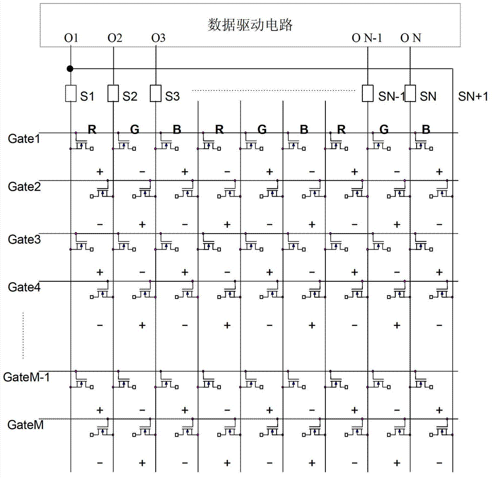
[0086] Figure 4 is a schematic diagram of a circuit structure of a liquid crystal display panel according to Embodiment 2 of the present invention. Figure 4 The arrangement structure of the sub-pixels in the circuit structure of the liquid crystal display panel shown is the same as figure 2 The arrangement structure of the sub-pixels in the circuit structure of the liquid crystal display panel shown is the same; Figure 4 The circuit structure of the liquid crystal display panel shown with figure 2 The circuit structure of the shown LCD panel is different in that, figure 2 The middle data driving circuit is directly connected with the N+1 data lines and provides the pixel voltage, and Figure 4 The middle data drive circuit is not directly connected to the N+1 data lines and provides pixel voltages, but is connected to the N+1 data lines through a switch control circuit to provide pixel voltages.

[0087] like Figure 4 The preferred embodiment shown, the preferred e...

Embodiment 3

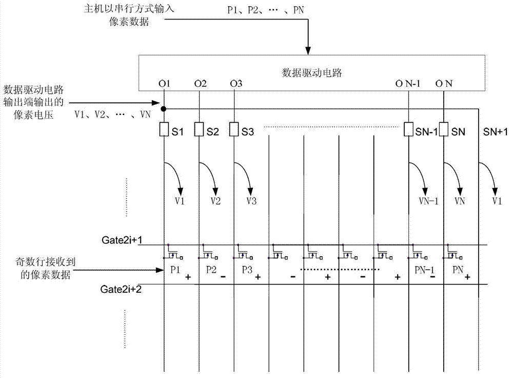
[0104] Image 6 is a schematic diagram of the circuit structure of the liquid crystal display panel according to the third embodiment of the present invention.

[0105] like Image 6 As shown, the application provides a liquid crystal display panel, which includes:

[0106] A plurality of sub-pixels, the plurality of sub-pixels are arranged in a matrix of M rows×N columns;

[0107] N+1 parallel data lines S1, S2, ... , SN, SN+1, each data line is used to receive and transmit pixel data;

[0108] And M scanning lines Gate1, Gate2, . . . , GateM-1, GateM perpendicularly intersecting each data line.

[0109]Wherein, each sub-pixel is arranged at the intersection of the scan line and the data line and coupled with the scan line and the data line. Specifically, each sub-pixel includes a pixel electrode (not shown in the figure) and a TFT (thin film transistor, thin film transistor) as a pixel switch. The above-mentioned "coupling" means that the pixel electrode and the drain of...


PUM


Abstract

The invention discloses a liquid crystal display panel and a liquid crystal display. The liquid crystal display panel comprises sub-pixels, N+1 data lines and M scanning lines; the sub-pixels are arranged according to the matrix way of M rows by N columns; every data line receives pixel data; the M scanning lines are intersected with the data lines to form the pixel area; a grid electrode of the <i+1>th sub-pixel which is in coupling connection with the first data line is in coupling connection with the <2i+1>th scanning line; a grid electrode of the <i+1>th sub-pixel which is in coupling connection with the <i+2>th data line is in coupling connection with the <i+1>th scanning line; a grid electrode of the <i+1>th sub-pixel which is in coupling connection with the <n+1>th data line is in coupling connection with the <2i+2>th scanning line; the first data line and the <n+1>th data line are connected at the pixel data received end; I is a nonnegative integer which is smaller than or equal to n-2. According to the liquid crystal display panel and the liquid crystal display, the design that a data driving circuit does not need to be changed can be achieved and the cost is reduced.

Description

technical field [0001] The present invention relates to the technical field of liquid crystal display, in particular, to a liquid crystal display panel and a liquid crystal display device. Background technique [0002] The inversion modes of the polarity transformation of the display panel in the prior art may include the following four modes: frame inversion mode, row inversion mode, column inversion mode, and dot inversion mode, wherein the dot inversion mode is used for The source driver consumes the most power, but displays the best results. [0003] figure 1 It is a schematic layout diagram of a circuit connection of a display panel according to the related prior art. [0004] Specifically, the circuit arrangement structure on the liquid crystal display panel in the prior art adopts such as figure 1 As shown in the zigzag structure, implementing this structure in a display panel can achieve a dot inversion display effect in a column inversion driving manner. The pri...

Claims


Application Information

Patent Timeline
Patent Type & Authority Applications(China)
IPC IPC(8): G02F1/1362G02F1/133G09G3/36
Inventor 李元范松曾章和黄建才
Owner SHANGHAI TIANMA MICRO ELECTRONICS CO LTD
Why Eureka
Try Eureka