Top grid type TFT array substrate, manufacturing method thereof, display panel and display device

An array substrate, top grid type technology, applied in nonlinear optics, instruments, optics, etc., can solve the problems of small aperture ratio of display panels, low image contrast, reduced aperture ratio of display panels, etc., to ensure display characteristics, overcome Alignment misalignment, reducing the effect of increased size

Inactive Publication Date: 2014-02-19
HEFEI BOE OPTOELECTRONICS TECH +1
View PDF5 Cites 11 Cited by
  • Summary
  • Abstract
  • Description
  • Claims
  • Application Information

AI Technical Summary

Problems solved by technology

[0005] The invention provides a top-gate TFT array substrate and a manufacturing method thereof, which are used to solve the problem in the prior art that the aperture ratio of the display panel is severely reduced when the black matrix is ​​enlarged to prevent light leakage at the edge of the display area.
[0006] The present invention also provides a display panel to solve the problem of a small aperture ratio of the display panel
[0007] At the same time, the present invention also provides a display device to solve the problem of low image contrast on the display screen of the display device

Method used


Image

  • Top grid type TFT array substrate, manufacturing method thereof, display panel and display device
  • Top grid type TFT array substrate, manufacturing method thereof, display panel and display device
  • Top grid type TFT array substrate, manufacturing method thereof, display panel and display device

Examples


Embodiment 1

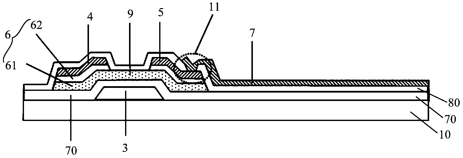
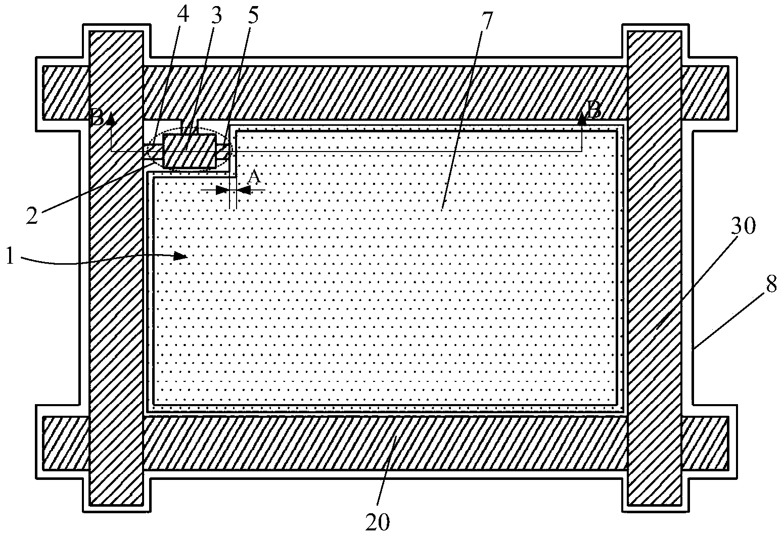
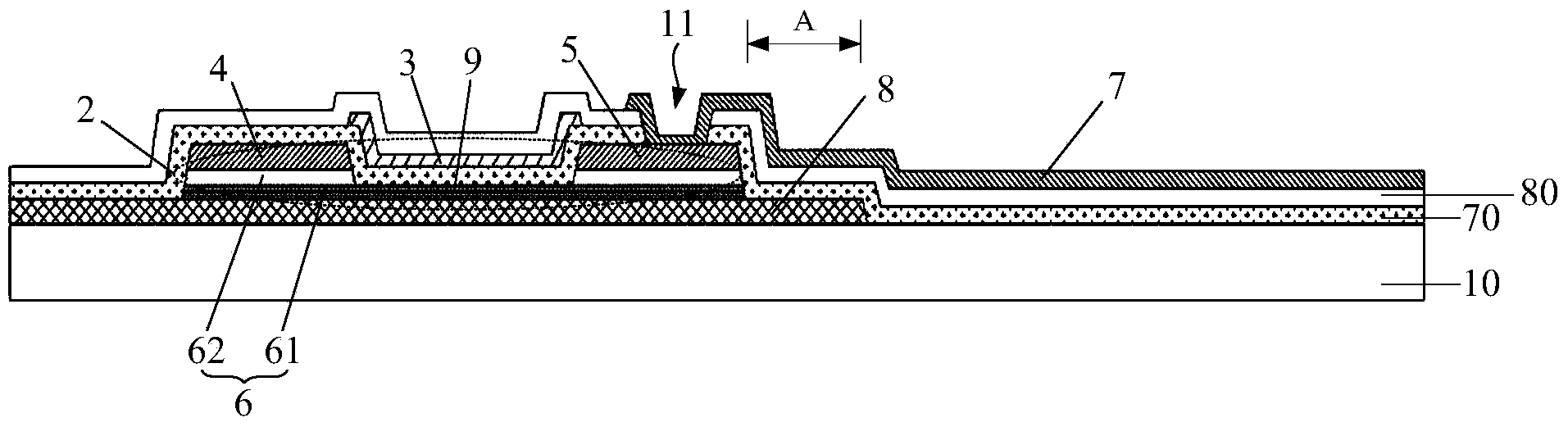
[0022] combine figure 2 with image 3 As shown, a top-gate TFT array substrate is provided in an embodiment of the present invention, which includes a base substrate 10, gate lines 20 and data lines 30 formed on the base substrate 10, and gate lines 20 and data lines 30 A defined pixel unit 1 includes a top-gate TFT 2 and a pixel electrode 7 . Among them, TFT2 (TFT in the following content refers to top-gate TFT) includes active layer pattern 6, source electrode 4 and drain electrode 5, gate insulating layer 70, gate electrode 3 and passivation layer formed on base substrate 10 in sequence. The active layer 6 includes a TFT channel 9 located between the source electrode 4 and the drain electrode 5 . The pixel electrode 7 is connected to the drain electrode 5 through the passivation layer via hole 11 . For the top-gate TFT array substrate, the gate insulating layer 70 and the passivation layer 80 can protect the TFT channel 9 from the influence of external light and ensure ...

Embodiment 2

[0027] The present embodiment provides a display panel, specifically a liquid crystal display panel, which includes a color filter substrate and an array substrate arranged opposite to each other, and a liquid crystal layer filled between the color filter substrate and the array substrate. Thin film transistors and pixel electrodes are formed on the array substrate. The thin film transistor is used as a switching device to control and generate an electric field that drives the deflection of the liquid crystal molecules to realize the display of the screen.

[0028] Among them, the array substrate adopts the top-gate TFT array substrate in Embodiment 1, that is, the black matrix of the display panel is formed on the array substrate, which overcomes the alignment deviation problem that occurs when the array substrate and the color filter substrate are aligned, and increases the black matrix. The size of the matrix ensures no light leakage at the edge of the display area, effecti...

Embodiment 3

[0030] This embodiment provides a display device, specifically a liquid crystal display device. The display panel of the display device adopts the display panel in Embodiment 2. The increase in the aperture ratio of the display panel improves the contrast of the display screen of the display device and ensures The picture display quality of the display device.


PUM


Abstract

The invention relates to the technical field of displaying, and discloses a top grid type TFT array substrate, a manufacturing method of the top grid type TFT array substrate, a display panel and a display device. A black matrix of the display panel is formed on the array substrate and located below a TFT, an overlapped area exists between the black matrix and a pixel electrode, the alignment deflection problem produced when the array substrate and a color film substrate are folded together is solved, it is ensured that light leakage does not occur in the edge of the display area when the size of the black matrix is increased, meanwhile, the increased size of the black matrix is effectively reduced, the opening rate of the display panel is increased, and the display characteristic of the display device is ensured.

Description

technical field [0001] The invention relates to the field of display technology, in particular to a top-gate TFT array substrate and a manufacturing method thereof, a display panel and a display device. Background technique [0002] Thin Film Transistor Liquid Crystal Display (TFT-LCD for short) is an important flat panel display device. Its main structure is an array substrate and a color filter substrate arranged in a pair of boxes, and the array substrate and color filter substrate are filled with liquid crystal layer between the substrates. Gate lines and data lines and pixel units defined by the gate lines and data lines are formed on the array substrate, and each pixel unit includes a thin film transistor (Thin Film Transistor, TFT for short) and a pixel electrode. During the display process, the TFT is used as a switch to control the application of a driving electric field to the liquid crystal, thereby controlling the rotation of the liquid crystal and realizing the...

Claims


Application Information

Patent Timeline
Patent Type & Authority Applications(China)
IPC IPC(8): G02F1/1368
Inventor 郭霄吕凤珍储松南张新霞
Owner HEFEI BOE OPTOELECTRONICS TECH
Why Eureka
Try Eureka