Radio frequency switching circuit of III-V group MOSFET device

A III-V, radio frequency switch technology, applied in the direction of electronic switches, electrical components, pulse technology, etc., can solve the problems that it is difficult to reach the optimal DC bias point of the switching system, and the chip space area cannot be fully utilized, and achieve low DC Effects of power consumption, improved dynamic range, and improved integration

Inactive Publication Date: 2014-02-19
INST OF MICROELECTRONICS CHINESE ACAD OF SCI
View PDF6 Cites 8 Cited by
  • Summary
  • Abstract
  • Description
  • Claims
  • Application Information

AI Technical Summary

Problems solved by technology

[0003] On the other hand, in civil radio frequency communication, due to the limited voltage provided by the DC voltage source, it is often difficult to reach the optimal DC bias point for the switching system. Therefore, it is necessary to boost the DC bias circuit. Common boost circuits generally Using CMOS technology, there is a compatibility problem with the traditional GaAs technology. At the same time, the circuit generally places the boost circuit on the periphery, which fails to make full use of the chip space area.

Method used


Image

  • Radio frequency switching circuit of III-V group MOSFET device

Examples


Embodiment Construction

[0022] In order to make the object, technical solution and advantages of the present invention clearer, the present invention will be described in further detail below in conjunction with specific embodiments and with reference to the accompanying drawings.

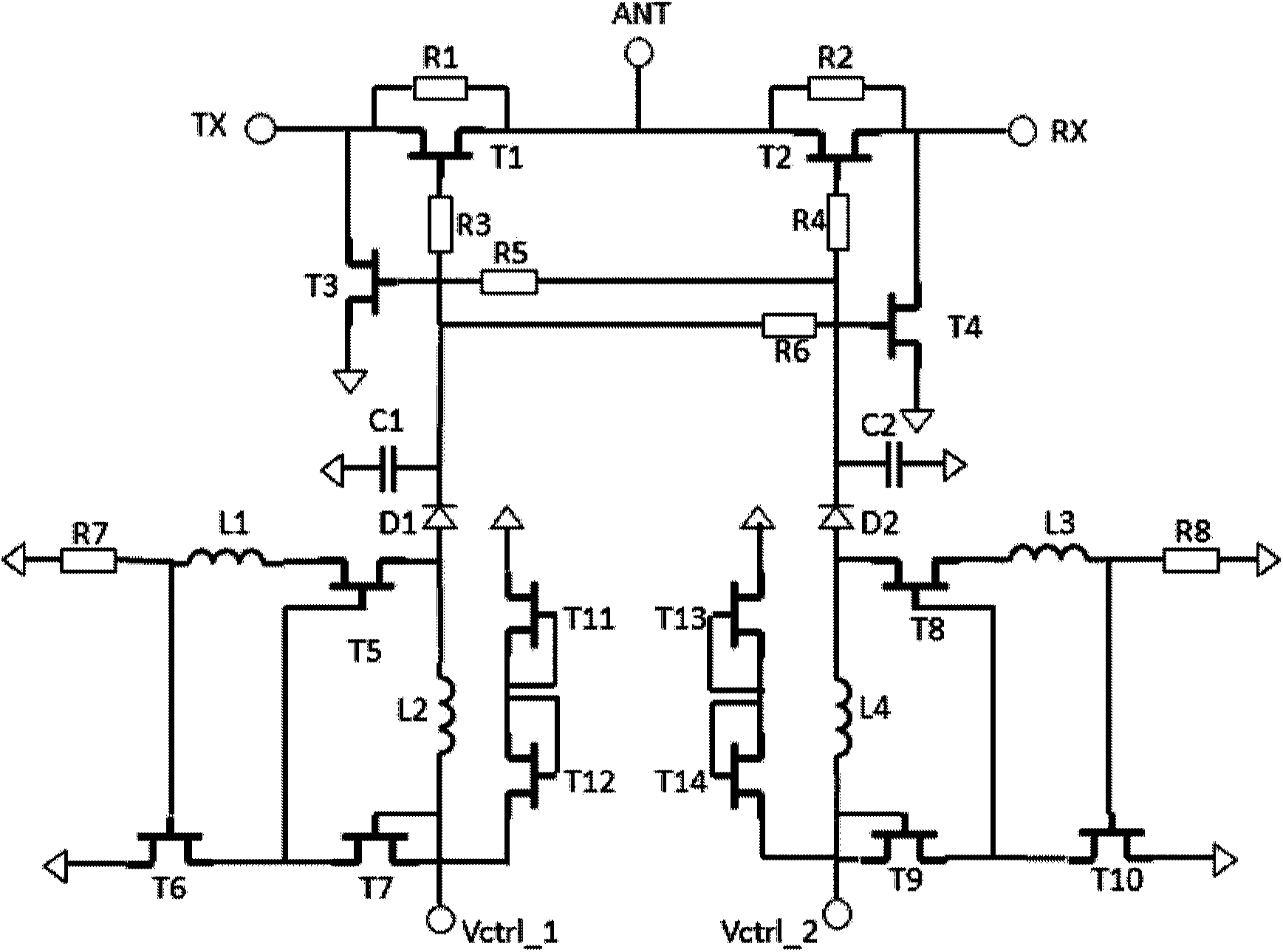
[0023] Such as figure 1 as shown, figure 1 The structure schematic diagram of the radio frequency switch circuit of the III-V group MOSFET device provided for the present invention, this radio frequency switch circuit comprises a self-bias switch circuit made of GaAs MOSFET, this self-bias switch circuit is a radio frequency signal path, has two DC voltage bias terminal, each DC voltage bias terminal is connected with an electrostatic protection circuit to prevent the switch from being damaged due to the large voltage brought by static electricity; at the same time, each DC voltage bias terminal is also connected with a self-rising The voltage circuit is used to boost the DC power supply voltage.

[0024] The self-bias ...


PUM


Abstract

The invention discloses a radio frequency switching circuit of a III-V group MOSFET device. The radio frequency switching circuit comprises an automatic biasing switching circuit formed by a GaAs MOSFET, the automatic biasing switching circuit is a radio frequency signal channel and is provided with two direct current voltage biasing ends, and each direct current voltage biasing end is connected with an electrostatic protection circuit and used for preventing the switch from being damaged due to the large voltages brought about by static electricity. Meanwhile, each direct current voltage biasing end is further connected with a self boosted circuit and used for boosting of direct current supply voltages. According to the radio frequency switching circuit, the GaAs MOSFET device is used for being manufactured into the switching circuit, the radio frequency switching speed is increased, meanwhile, the gate dynamic range is expanded, low insertion loss is achieved, and the integration of a traditional radio frequency switch is improved.

Description

technical field [0001] The invention relates to the technical field of radio frequency integrated circuits, in particular to a radio frequency switch circuit of III-V MOSFET devices. Background technique [0002] In practical RF switch applications, electrostatic problems have always been one of the factors that cannot be ignored. Because static electricity will bring a short and large voltage, it is extremely easy to cause the switch to fail under strong voltage. Therefore, the electrostatic protection circuit has always been an important factor that needs to be considered by RF switch designers. [0003] On the other hand, in civil radio frequency communication, due to the limited voltage provided by the DC voltage source, it is often difficult to reach the optimal DC bias point for the switching system, so it is necessary to boost the DC bias circuit. Common boost circuits generally The use of CMOS technology has compatibility problems with traditional GaAs technology. ...

Claims


Application Information

Patent Timeline
Patent Type & Authority Applications(China)
IPC IPC(8): H03K17/687
Inventor 刘洪刚杨靖治常虎东刘桂明
Owner INST OF MICROELECTRONICS CHINESE ACAD OF SCI
Why Eureka
Try Eureka