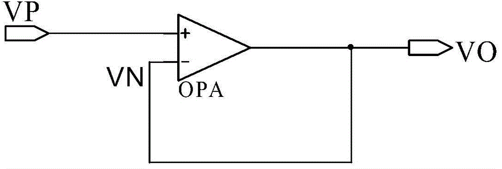
voltage follower circuit
A voltage-following circuit and voltage technology, applied in the circuit field, can solve problems such as large mismatch voltage, low gate input current, and large base current
- Summary
- Abstract
- Description
- Claims
- Application Information
AI Technical Summary
Problems solved by technology
Method used
Image

Examples
Embodiment Construction
[0031] In order to make the object, technical solution and advantages of the present invention clearer, the present invention will be further described in detail below in conjunction with the accompanying drawings. Obviously, the described embodiments are only some embodiments of the present invention, rather than all embodiments . Based on the embodiments of the present invention, all other embodiments obtained by persons of ordinary skill in the art without making creative efforts belong to the protection scope of the present invention.
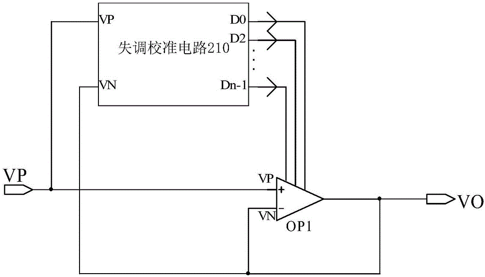
[0032] figure 2 A schematic structural diagram of a voltage follower circuit provided by an embodiment of the present invention. like figure 2 As shown, the voltage follower circuit includes: an offset calibration circuit 210 and a programmable operational amplifier OP1.
[0033] The input terminals of the offset calibration circuit 210 are respectively connected to the first input terminal and the second input terminal of the programm...
PUM
 Abstract
Description
Claims
Application Information
 - R&D
- Intellectual Property
- Life Sciences
- Materials
- Tech Scout
- Unparalleled Data Quality
- Higher Quality Content
- 60% Fewer Hallucinations
Browse by: Latest US Patents, China's latest patents, Technical Efficacy Thesaurus, Application Domain, Technology Topic, Popular Technical Reports.
© 2025 PatSnap. All rights reserved.Legal|Privacy policy|Modern Slavery Act Transparency Statement|Sitemap|About US| Contact US: help@patsnap.com