Impedance matching method of plasma etching system

An etching system, plasma technology, applied in semiconductor/solid-state device manufacturing, discharge tubes, electrical components, etc., can solve problems such as low efficiency of frequency modulation algorithm and inability to automatically find matching frequencies

Active Publication Date: 2014-03-12
ADVANCED MICRO FAB EQUIP INC CHINA
View PDF4 Cites 14 Cited by
  • Summary
  • Abstract
  • Description
  • Claims
  • Application Information

AI Technical Summary

Problems solved by technology

In the existing method of adjusting the frequency of the source power to achieve impedance matching, the frequency modulation algorithm of the source power is inefficient and cannot automatically find a suitable matching frequency

Method used


Image

  • Impedance matching method of plasma etching system
  • Impedance matching method of plasma etching system

Examples


Embodiment Construction

[0027] According to the description in the background art, the impedance matching efficiency of the plasma etching system in the prior art is low.

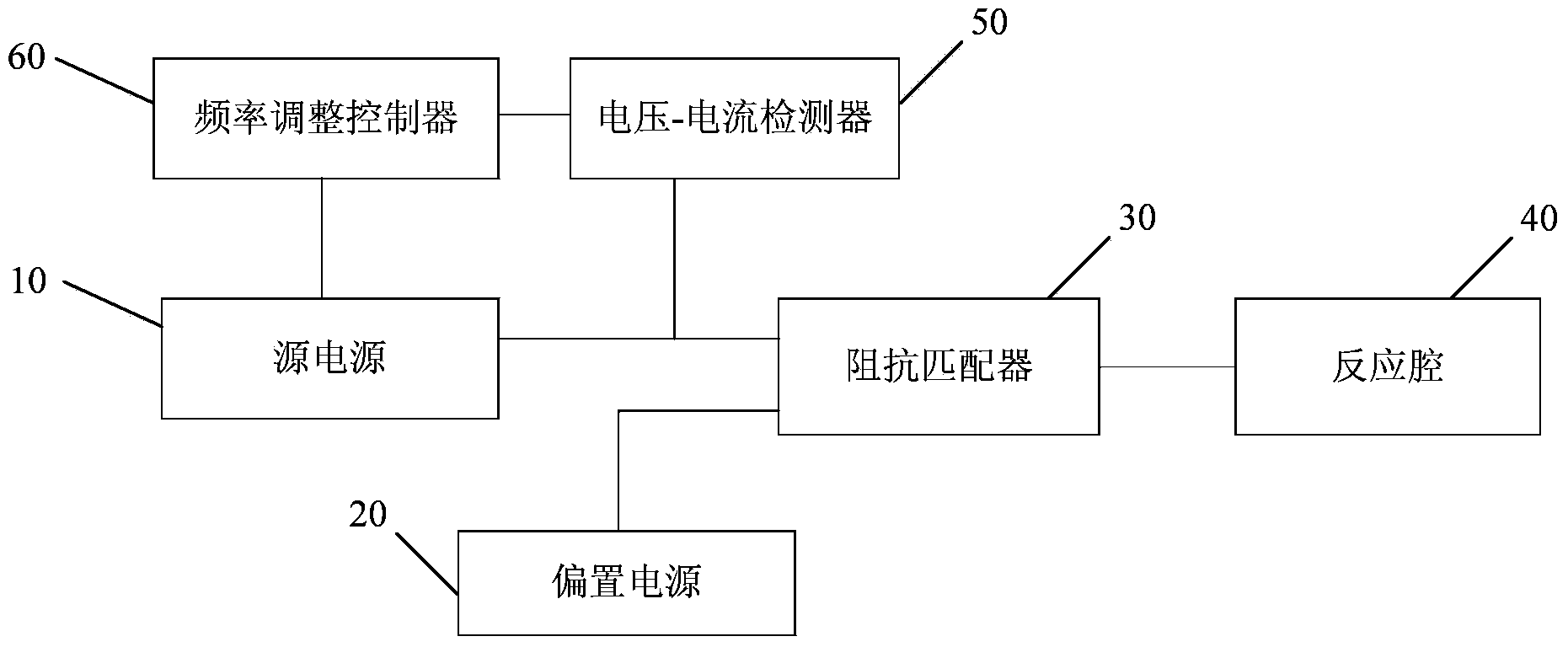
[0028] Since the source power supply is used to generate the plasma in the reaction chamber, the frequency of the source power supply has a great influence on the impedance of the plasma, while the frequency change of the bias power supply has little influence on the impedance of the plasma, so it can be adjusted by adjusting The frequency of the source power is used to find a suitable matching frequency to achieve impedance matching.

[0029] Since the bias power supply is in the state of pulse on and pulse off, the impedance of the system is quite different. At the moment when the bias power supply switches from the pulse-on state to the pulse-off state, the impedance of the output end of the impedance matching device changes, which will lead to an increase in the reflection coefficient of the power supply, which triggers a roug...


PUM


Abstract

The invention relates to an impedance matching method of a plasma etching system. The impedance method comprises the steps of providing a plasma etching system, wherein the plasma etching system comprises an impedance matching device, the input end of the impedance matching device is electrically connected with a source power and a bias power supply, the output end of the impedance matching device is electrically connected with a reaction cavity, the end, connected with the source power, of the impedance matching device is electrically connected with one end of a voltage-current detector, and the other end of the voltage-current detector is connected with the source power through a frequency regulation control unit; the source power and the bias power supply simultaneously work under a continuous power mode, and a first matching frequency can be obtained by adjusting the frequency of the source power; the bias power supply is converted into a pulse power mode, and the first matching frequency serves as a benchmark frequency of the source power under a bias power supply pulse opening state, and when the bias power supply is converted to a pulse closing state from the pulse opening state, the benchmark frequency is adopted as the benchmark, so that a second matching frequency can be obtained by increasing or reducing the frequency of the source power.

Description

technical field [0001] The invention relates to the technical field of semiconductors, in particular to an impedance matching method of a plasma etching system. Background technique [0002] In the semiconductor process, processes related to plasma gas are becoming more and more important in the manufacture of semiconductor devices, such as plasma etching process, reactive ion etching process and so on. [0003] A dual-frequency plasma etching system generally includes an etching chamber, a bias power supply (bias power) and a source power supply (source power). The plasma is generated and maintained inside and is used to control the density of the plasma. The frequency of the bias power supply is low, typically a 2Mhz RF power supply, which is used to control the direction of movement of the plasma and the energy it carries. The bias power supply and the source power supply provide radio frequency power to the reaction chamber through an impedance matcher. [0004] In the...

Claims


Application Information

Patent Timeline
Patent Type & Authority Applications(China)
IPC IPC(8): H01L21/02H01J37/32
CPCH01J37/32183
Inventor 崔强叶如彬徐蕾倪图强
Owner ADVANCED MICRO FAB EQUIP INC CHINA
Why Eureka
Try Eureka