Crossed annular aligning mark based on TSV (through silicon via) three-dimensional integration process

An alignment mark and cross-shaped technology, applied in the field of microelectronics, can solve problems such as inability to expose copper, small footprint of graphics, increase reliability of TSV three-dimensional integrated devices, etc., achieve high production efficiency, meet high-precision alignment requirements, Scientific and reasonable effect of graphic and structural design

Active Publication Date: 2014-03-12
珠海天成先进半导体科技有限公司
View PDF5 Cites 10 Cited by
  • Summary
  • Abstract
  • Description
  • Claims
  • Application Information

AI Technical Summary

Problems solved by technology

[0003] In order to overcome the deficiencies of the prior art, the present invention provides a cross-ring alignment mark based on TSV three-dimensional integration technology, which adopts a ring-shaped cross pattern and a through-hole structure, and the manufacturing process is compatible with the TSV through-hole manufacturing process, and does not require additional introduction of other processes The process has the advantages of low cost and high efficiency, and its pattern occupies a small area, and its size is smaller than the diameter of the TSV through hole. It solves the process defect that the back of the TSV through hole is thinned and cannot expose copper due to the "Loading" effect, and increases the TSV three-dimensional integration. Device reliability

Method used


Image

  • Crossed annular aligning mark based on TSV (through silicon via) three-dimensional integration process
  • Crossed annular aligning mark based on TSV (through silicon via) three-dimensional integration process
  • Crossed annular aligning mark based on TSV (through silicon via) three-dimensional integration process

Examples


Embodiment 1

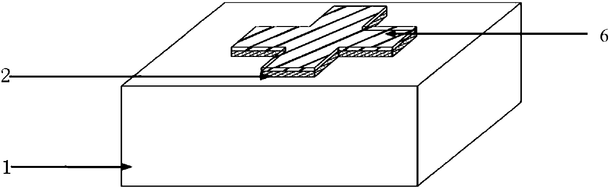
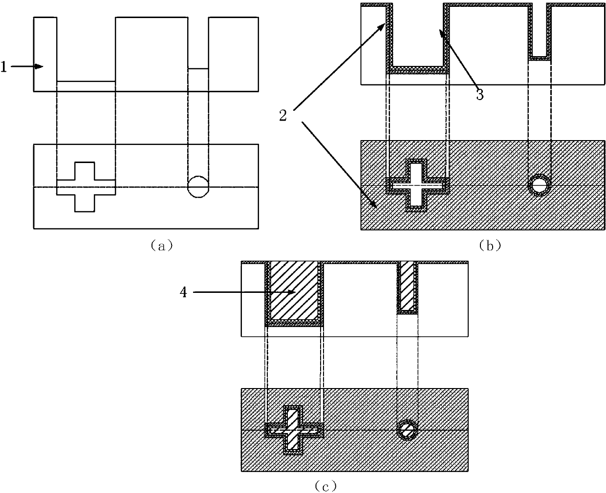
[0016] Such as Figure 4 As shown, when the TSV diameter W4 is 20 μm, the corresponding dimensions of the ring-shaped “ten” alignment mark are: L1 is 50 μm, L2 is 30 μm, W1 is 30 μm, and W2 is 30 μm. The size W3 of the annular "ten" opening is (L1-L2) / 2=10μm, the silicon dioxide insulating layer 2 filled inside is 1μm thick, and the tantalum nitride barrier layer / copper seed layer 3 is 0.5μm thick, of which tantalum nitride The thickness of the copper seed layer is 0.2 μm, the thickness of the copper seed layer is 0.3 μm, and the width of the filled copper pillar 4 is 8.5 μm.

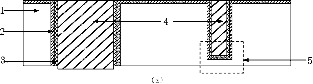
[0017] Such as Figure 5 As shown in , when aligning, register the solid "ten" alignment mark on the lithography board with the "ten" annular alignment mark on the wafer, and manually adjust the distance between the above two alignment marks through a contact lithography machine Dimensions W5 and W6, when both W5 and W6 are less than or equal to the registration accuracy of 0.4 μm, the pattern alignme...

Embodiment 2

[0019] Such as Figure 4 As shown, when the TSV diameter W4 is 30 μm, the corresponding dimensions of the ring-shaped “ten” alignment mark are: L1 is 40 μm, L2 is 20 μm, W1 is 40 μm, and W2 is 40 μm. The size W3 of the annular "ten" opening is (L1-L2) / 2=10μm, the silicon dioxide insulating layer 2 filled inside is 1μm thick, and the tantalum nitride barrier layer / copper seed layer 3 is 0.5μm thick, of which tantalum nitride The thickness of the copper seed layer is 0.2 μm, the thickness of the copper seed layer is 0.3 μm, and the width of the filled copper pillar 4 is 8.5 μm.

[0020] When aligning, register the "ten" ring alignment mark on the photolithography board with the "ten" ring alignment mark on the wafer, and manually adjust the distance between the above two alignment marks W5 and W6, when W5 and W6 are less than or equal to the registration accuracy of 0.5 μm, the pattern alignment is completed.

Embodiment 3

[0022] Such as Figure 4 As shown, when the TSV diameter W4 is 40 μm, the corresponding dimensions of the ring-shaped “ten” alignment mark are: L1 is 60 μm, L2 is 30 μm, W1 is 30 μm, and W2 is 30 μm. The size W6 of the annular "ten" opening is (L1-L2) / 2=15μm, the silicon dioxide insulating layer 2 filled inside is 1μm thick, the tantalum nitride barrier layer / copper seed layer 3 is 0.5μm thick, and the tantalum nitride The thickness of the copper seed layer is 0.2 μm, the thickness of the copper seed layer is 0.3 μm, and the width of the filled copper pillar 4 is 13.5 μm.

[0023] When aligning, register the "ten" ring alignment mark on the photolithography board with the "ten" ring alignment mark on the wafer, and manually adjust the distance between the above two alignment marks W5 and W6, when W5 and W6 are less than or equal to the registration accuracy of 0.6 μm, the pattern alignment is completed.


PUM


Abstract

The invention provides a crossed annular aligning mark based on a TSV (through silicon via) three-dimensional integration process. An annular blind hole is formed in a plane of the silicon wafer surface provided with a TSV through hole, the outer edge and the inner edge of the annular blind hole are respectively in crossed structures, in addition, the two crossed structures are coaxial, the width of the annular blind hole is smaller than the diameter W4 of the TSV through hole, the annular blind hole sequentially comprises a silicon dioxide simulation layer, a tantalum nitride blocking layer and a copper seed layer from outside to inside, and copper is filled inside the annular blind hole. The crossed annular aligning mark has the advantages that the additional introduction of other technical flow processes is not needed, the cost is low, the efficiency is high, and the like. In addition, the pattern occupation area is small, the dimension is smaller than the diameter of the TSV through hole, the technical defect of copper exposure incapability due to the TSV through hole backside thinning caused by the loading effect is overcome, and the reliability of TSV three-dimensional integration devices is improved.

Description

technical field [0001] The invention relates to the technical field of microelectronics. Background technique [0002] At present, wafers that require simultaneous TSV three-dimensional integration mostly use Stepper (stepping) lithography machines to complete the IC process, while TSV three-dimensional integration processes use contact lithography machines. The lithographic alignment marks required by the two are different. Therefore, the alignment marks must be converted when using the Stpper lithography machine to complete the IC process wafers for TSV three-dimensional integration. It is necessary to redesign the alignment marks with high recognition and scientific and reasonable structure. Only in this way can the contact lithography machine be quickly positioned and accurately registered, thereby reducing alignment deviation and ensuring the quality of TSV lithography and subsequent bonding processes. At present, the alignment mark in the TSV three-dimensional integra...

Claims


Application Information

Patent Timeline
Patent Type & Authority Applications(China)
IPC IPC(8): H01L23/544G03F9/00
Inventor 单光宝刘松孙有民袁海张巍
Owner 珠海天成先进半导体科技有限公司
Why Eureka
Try Eureka