LDMOS power transistor array structure and realization method of layout of LDMOS power transistor array structure

A technology of power transistor and array structure, applied in electric solid device, semiconductor device, special data processing application, etc., can solve the problem of LDMOS power transistor array reliability deterioration, environmental temperature rise, current distribution on-resistance cracking and cracking. And other issues

Inactive Publication Date: 2014-03-12
SHANGHAI HUAHONG GRACE SEMICON MFG CORP
View PDF4 Cites 6 Cited by
  • Summary
  • Abstract
  • Description
  • Claims
  • Application Information

AI Technical Summary

Problems solved by technology

The non-uniformity of current distribution causes the cracking of the on-resistance of the entire LDMOS power transistor array to be worse than that of a single LDMOS transistor
Makes the reliability of LDMOS power transistor array worse
[0005] In addition, the substrate current generated at the substrate (Pbody) of the traditional LDMOS power transistor array can be absorbed by the lead-out terminal (P-type heavily doped region) of the substrate at least through the length of lp. As mentioned above, a substrate ( Pbody) will receive substrate current from four directions, and compared with a single LDMOS transistor, the substrate current it receives will be four times larger, which will cause the parasitic NPN transistor of the LDMOS power transistor array to be turned on more easily under the same conditions
Moreover, due to the large current and high voltage flowing through the large LDMOS power transistor array during operation, its self-heating phenomenon will cause the ambient temperature of the LDMOS power transistor array to rise, and the parasitic NPN transistor is easier to turn on at high temperature

Method used


Image

  • LDMOS power transistor array structure and realization method of layout of LDMOS power transistor array structure
  • LDMOS power transistor array structure and realization method of layout of LDMOS power transistor array structure
  • LDMOS power transistor array structure and realization method of layout of LDMOS power transistor array structure

Examples


Embodiment Construction

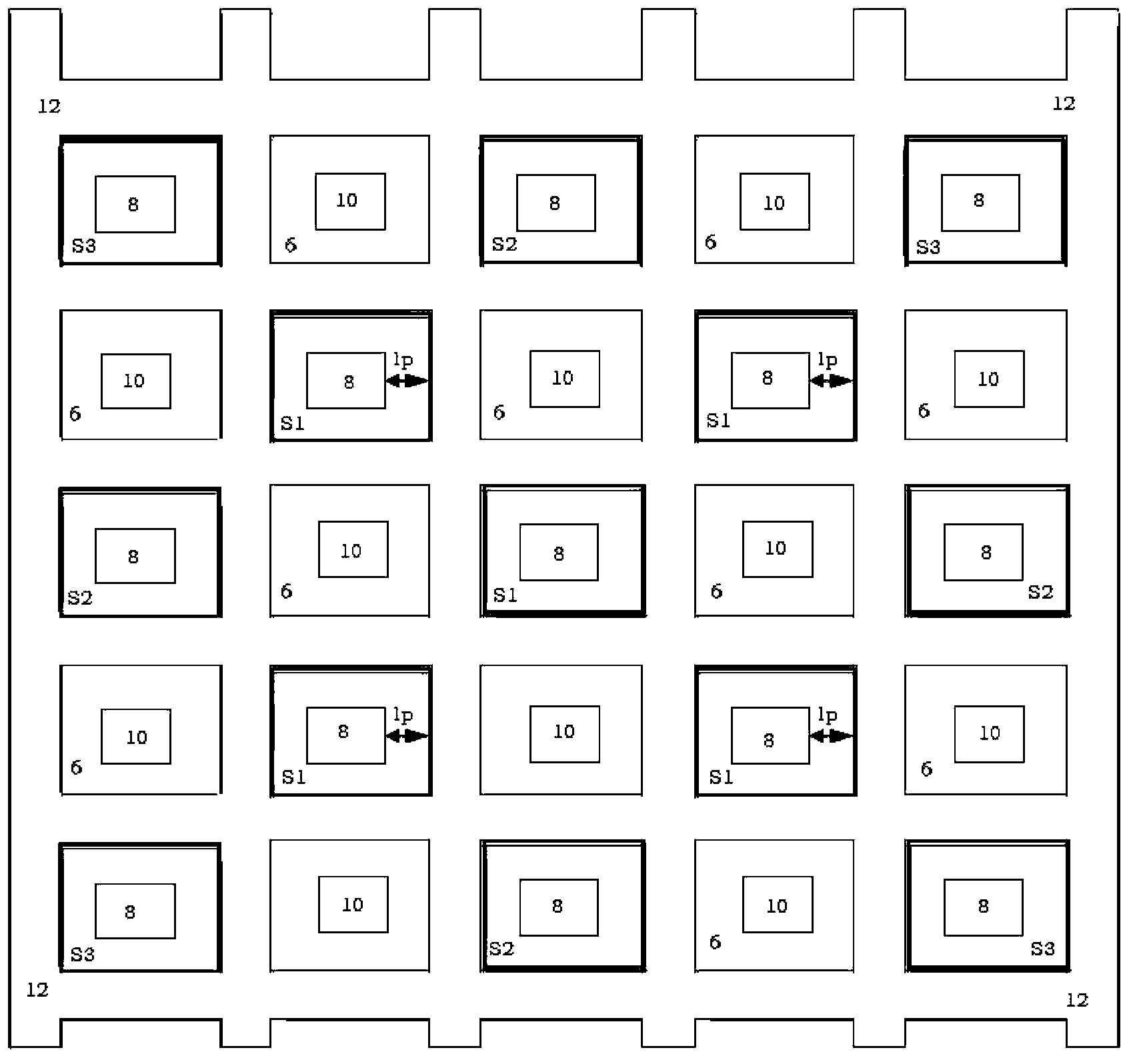
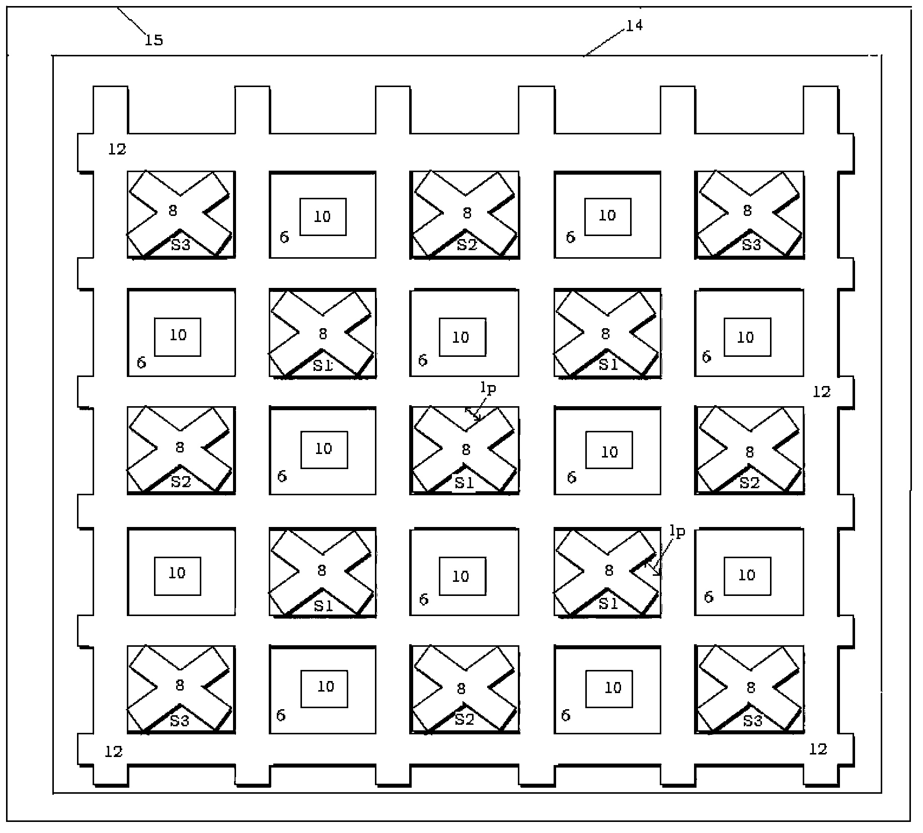
[0034] Such as figure 2 As shown, an embodiment of the LDMOS power transistor array structure of the present invention includes: a plurality of parallel-connected LDMOS transistors, and adjacent LDMOS transistors share a source or drain connection, wherein the sources and substrate terminals of all LDMOS transistors The drains are connected in parallel through metal lines, and the substrate terminal of each LDMOS transistor (i.e. image 3 The P-type heavily doped region 8) is arranged in an X-shaped cross manner, and there is a separate drain at the outermost periphery of the power transistor array to form a drain guard ring that is drawn out through metal lines, and an isolation ring is provided outside the drain guard ring .

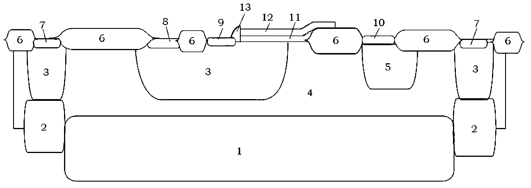
[0035] Such as image 3 As shown, each LDMOS transistor in this embodiment includes: an N-type epitaxial layer 1 formed on a P-type substrate, a P-type buried layer 2 and an N-type buried layer 4 formed on the N-type epitaxial layer 1, wherein The ...


PUM


Abstract

The invention discloses an LDMOS power transistor array structure comprising multiple LDMOS transistors which are identical in structure and connected in parallel. The adjacent LDMOS transistors are connected by sharing a source electrode or a drain electrode. The source electrodes and substrate lead-out ends of all the LDMOS transistors are connected in parallel via metal wires, and the drain electrodes are connected in parallel via the metal wires. The substrate lead-out end of each LDMOS transistor is arranged by adopting an X-shaped cross mode. The outmost periphery of a power transistor array is provided with the single drain electrode so that a drain electrode protective ring is formed and led out via the metal wires. The external side of the drain electrode protective ring is also provided with an isolating ring so that other devices are isolated. The invention also discloses a realization method of a layout of the LDMOS power transistor array structure. Reliability of the power transistor array can be enhanced (e.g. the HIC service life of the power transistor array is enhanced, safety working range of the power transistor array is enlarged, etc.) by the LDMOS power transistor array structure without changing technology.

Description

technical field [0001] The invention relates to the field of semiconductor manufacturing, in particular to an LDMOS power transistor array structure. The invention also relates to a layout realization method of the LDMOS power transistor array structure. Background technique [0002] In the BCD process, it can withstand high voltage and high current. LDMOS (Laterally Diffused Metal Oxide Semiconductor) is usually used as a switch tube application as the final output driver. In order to provide a sufficiently large drive current, a power transistor array composed of multiple LDMOS parallel connections is usually used. The on-resistance is the most important performance index of this power transistor array, and the life of HCI (that is, hot carrier effect) and Safe Operating Area (SOA) is the most important reliability indicator for power transistor arrays. For example, the power transistor array will work under the conditions of high voltage (such as 24V) and high current d...

Claims


Application Information

Patent Timeline
Patent Type & Authority Applications(China)
IPC IPC(8): H01L27/02G06F17/50
Inventor 仲志华
Owner SHANGHAI HUAHONG GRACE SEMICON MFG CORP
Why Eureka
Try Eureka