Method for designing high-safety chip active shielding physical protection structure

A protection structure and security chip technology, applied in computing, electrical digital data processing, special data processing applications, etc., can solve the problem of particle contamination and failure of active shielding layer

Inactive Publication Date: 2014-03-19
BEIJING CEC HUADA ELECTRONIC DESIGN CO LTD
View PDF4 Cites 20 Cited by
  • Summary
  • Abstract
  • Description
  • Claims
  • Application Information

AI Technical Summary

Problems solved by technology

The variable pitch active shielding physical protection structure proposed by the present invention can effectively sol

Method used


Image

  • Method for designing high-safety chip active shielding physical protection structure
  • Method for designing high-safety chip active shielding physical protection structure

Examples


Embodiment Construction

[0014] The method disclosed in the present invention will be described in detail below in conjunction with the accompanying drawings.

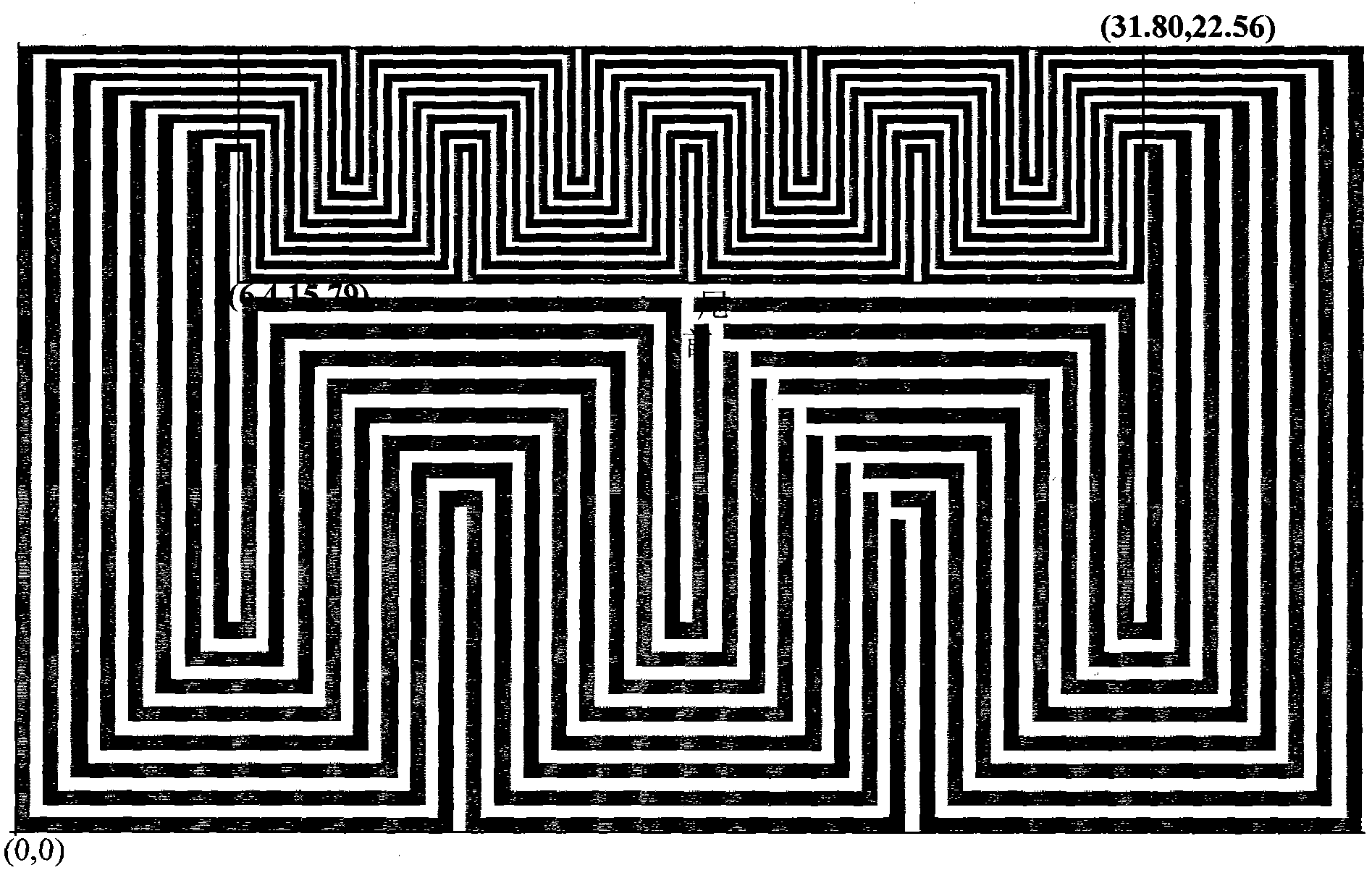
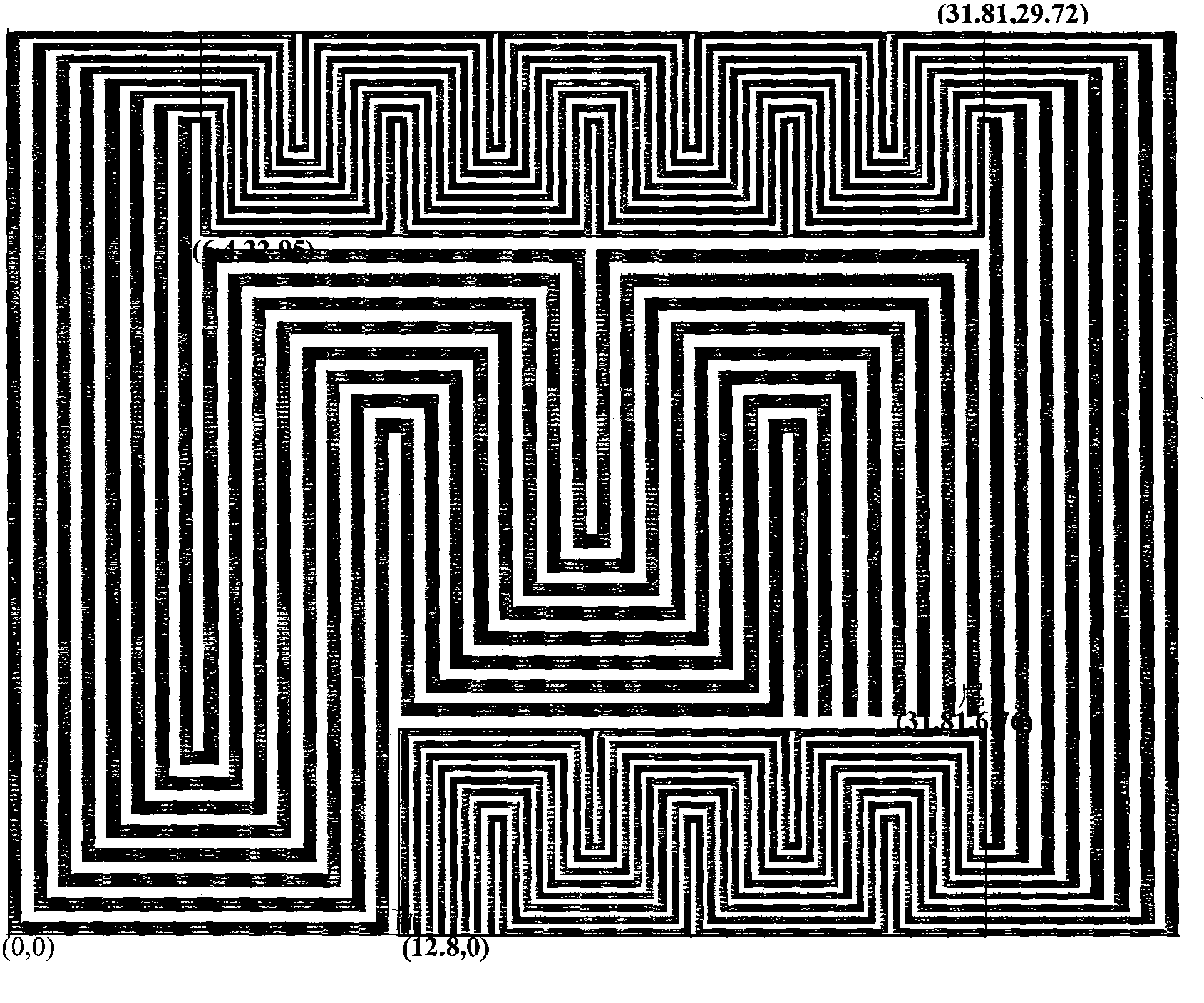
[0015] Such as figure 1 As shown, the chip is divided into a high-security area and a non-high-security area. There are 8 shielded wires in total, and the 8 active shields in the high-security area adopt pitch=0.4um (where width=0.2um, spacing=0.2um); the 8 active shields in the non-high-security area adopt pitch=0.8um (where width=0.4um, spacing=0.4um). The total area of ​​the instance area is 38um*22.56um; the origin of the coordinates of the instance area is the lower left corner, in which the high security area is a rectangular area, the coordinates of the lower left corner and the upper right corner are (6.4, 15.79), (31.8, 22.56), and the rest are non-high security area. The head and tail of the first shielded wire of the active shielded wire are hidden in the shielded wire area, and the coordinates are (19.2, 14.59) and (19.2, 14.99)...


PUM


Abstract

The invention provides a method for designing a high-safety chip active shielding physical protection structure. The chip active physical protection structure has the function that a high-safety chip is prevented from being attacked in an intrusive mode, for example the high-safety chip is tampered or detected in a physical mode. Single-layer metal wires are active shielding wires and the active shielding wires are fully distributed on the surface of the chip. In order to protect a lower-layer physical pattern against attack, the smallest design rule is usually adopted by the metal wires. If patterns designed according to the smallest rule are fully distributed on the chip, the possibility that the chip circuit functional performance failure caused by particle contamination is increased. In order to reduce the volume production chip circuit failure, the width and/or the spacing of the active shielding wires are/is usually widened. If the size of each active shielding wire is widened, the safety of the chip can be reduced. In order to solve the problem of the contradiction between the safety of the chip and the yield of the volume production products, the pitch-variable active shielding physical production structure is further provided, so that dual-improvement in the safety and the yield of the chip products is achieved.

Description

technical field [0001] The invention proposes a design method for an active shielding physical protection structure of a high-safety chip. The invention is suitable for the field of integrated circuit design with high security requirements. Background technique [0002] There are many attack methods for chip security, which can be roughly divided into three categories: non-intrusive attack, semi-intrusive attack, and intrusive attack. Intrusive attacks are also called physical attacks, and usually use tools and methods in chip reverse engineering to remove chip packages, extract layouts, and cut / connect circuits. Adding an active shielding layer on the top layer of the chip has a better defense effect against physical detection and attacks that tamper with some functions of the chip. When the connection of the active shielding layer is physically tampered or detected, the signal transmitted in the active shielding line will change after the chip is powered on, and the acti...

Claims


Application Information

Patent Timeline
IPC IPC(8): G06F17/50
Inventor 张颖潘亮陈波涛
Owner BEIJING CEC HUADA ELECTRONIC DESIGN CO LTD
Why Eureka
Try Eureka