A large current igbt layout with uniform grid voltage distribution

A technology of uniform distribution and gate voltage, applied in electrical digital data processing, instruments, calculations, etc., can solve the problems of inability to turn on the same voltage, inconsistent turn-on speed, and high local turn-on voltage, achieve uniform current distribution, speed up the turn-on speed, The effect of improving the opening speed

Active Publication Date: 2017-10-31
INST OF MICROELECTRONICS CHINESE ACAD OF SCI
View PDF5 Cites 0 Cited by
  • Summary
  • Abstract
  • Description
  • Claims
  • Application Information

AI Technical Summary

Problems solved by technology

[0006] The technical problem to be solved by the present invention is to provide a high-current IGBT layout with evenly distributed gate voltage, which solves the problems in the prior art high-current IGBT layout that cannot have the same turn-on voltage, inconsistent turn-on speed, and local turn-on voltage is too high

Method used


Image

  • A large current igbt layout with uniform grid voltage distribution
  • A large current igbt layout with uniform grid voltage distribution

Examples


Embodiment Construction

[0014] Glossary:

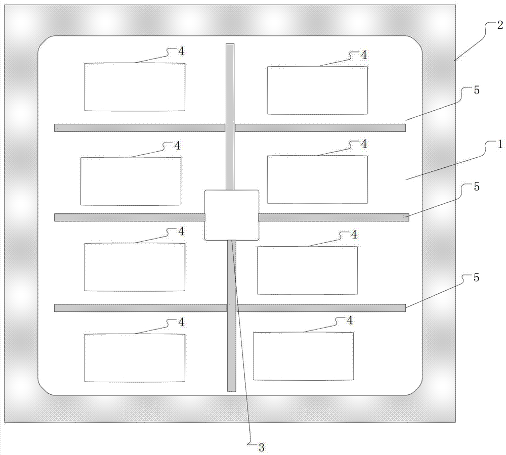
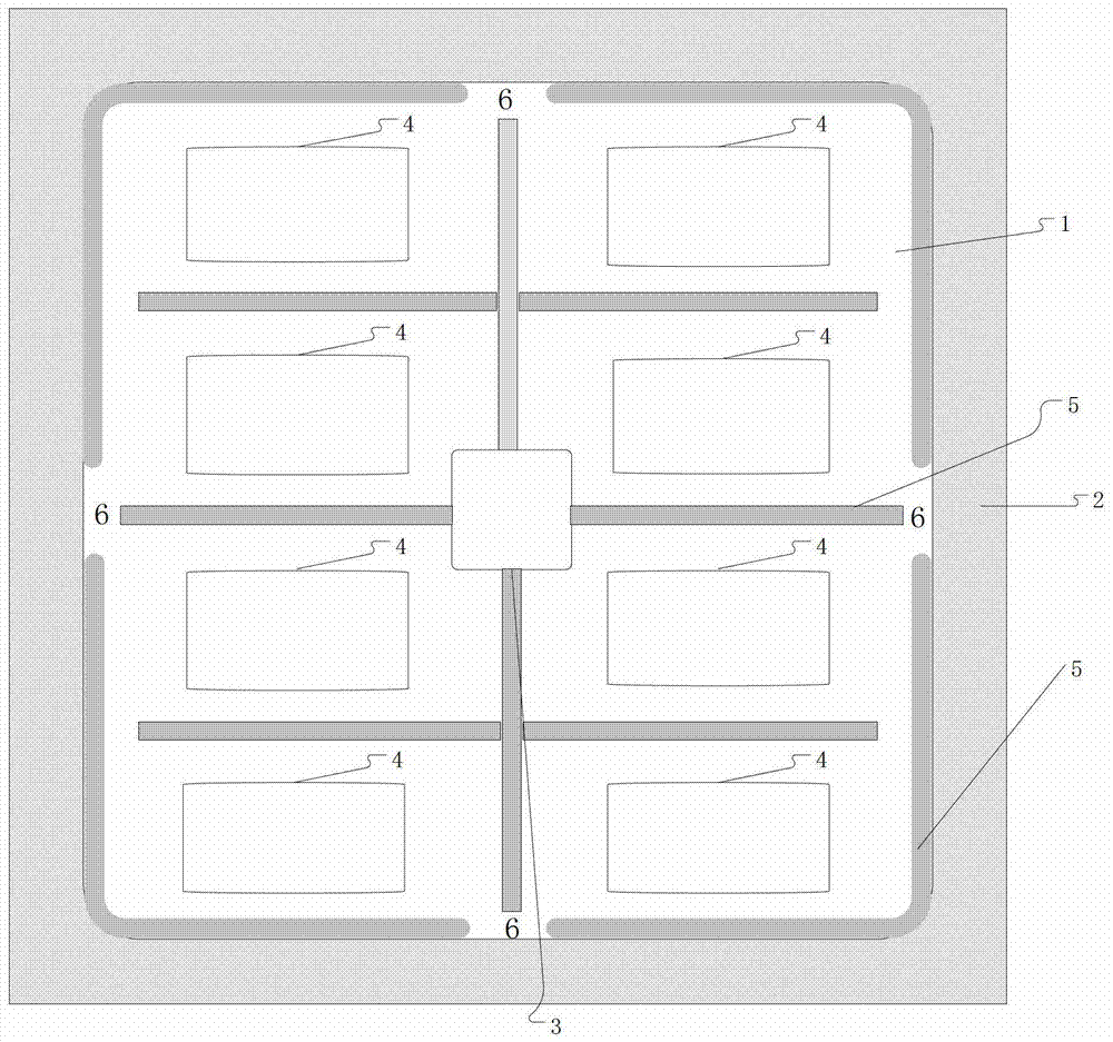
[0015] IGBT: Insulated Gate Bipolar Transistor

[0016] Cell area: the area formed by parallel connection of IGBT cells, which is equivalent to the active area.

[0017] Terminal area: It is located around the cell area and ensures the withstand voltage of the device.

[0018] Gatebus: In order to reduce the influence of the distribution resistance of the gate electrode material, polysilicon and metal are usually used to lead the potential of the gate pad to the cell unit far away from the pad, and Gatebus is the poly under the gate pad to extend to In the cell area between the source pads, there is an oxide layer (gate oxide) on the poly layer, the metal aluminum (AL) on the oxide layer, and the passivation layer (SIN) on the metal aluminum. Metal aluminum is connected to poly through the holes carved in the oxide layer to achieve equipotentiality.

[0019] see figure 2 , the embodiment of the present invention provides a large-current IGBT layout with...


PUM


Abstract

The invention discloses a high-current IGBT (insulated gate bipolar transistor) map with uniformly distributed grid voltage, and belongs to the technical field of semiconductors. The high-current IGBT map comprises a cellular area, a terminal area, gate buses, source voltage welding points and grid voltage welding points, the terminal area surrounds the cellular area, the source voltage welding points are arranged on the cellular area, the grid voltage welding points are arranged at the center of the source voltage welding points, the gate buses are arranged between the source voltage welding points as well as between the source voltage welding points and the grid voltage welding points. More than one disconnected gate buses are arranged at the joint of the cellular area and the terminal area. By the high-current IGBT map, the problem that grid cut-in voltage in existent map design schemes is in non-uniform distribution is solved, sufficient cutting-in of cells in the whole cellular area is guaranteed, and current distribution is uniform; meanwhile, cut-in speed of the cells in the integral cellular area is accelerated, and device cut-in speed is also increased.

Description

technical field [0001] The invention belongs to the technical field of semiconductors, in particular to a layout of a large current IGBT with evenly distributed grid voltage. Background technique [0002] The full name of IGBT is Insulate Gate Bipolar Transistor, which is an insulated gate bipolar transistor. It combines multiple advantages of MOSFET and GTR, and can meet the needs of high-voltage, high-current and other high-power devices, which greatly expands the application field of power semiconductor devices. As the main representative of new power electronic semiconductor devices, IGBT is widely used in the fields of industry, information, new energy, medicine, transportation, military and aviation. [0003] In terms of layout implementation, the IGBT device is composed of parallel cells, terminals, gate pads, source pads, etc. Therefore, the larger the current of the chip, the larger the corresponding chip area. In addition to the structure of the cell and the term...

Claims


Application Information

Patent Timeline
Patent Type & Authority Patents(China)
IPC IPC(8): G06F17/50
CPCY02E60/00
Inventor 左小珍朱阳军赵佳卢烁今田晓丽陆江吴振兴
Owner INST OF MICROELECTRONICS CHINESE ACAD OF SCI
Why Eureka
Try Eureka