
Enhanced FINFET process overlay mark

A technology for marking and marking areas, applied in the field of semiconductors, can solve the problems of not being able to fully meet the requirements of manufacturing non-planar devices

Active Publication Date: 2014-03-26
TAIWAN SEMICON MFG CO LTD
View PDF4 Cites 5 Cited by
  • Summary
  • Abstract
  • Description
  • Claims
  • Application Information

AI Technical Summary

Problems solved by technology

While existing overlay marks are often adequate for planar devices, existing overmarks are not fully adequate for fabricating non-planar devices

Method used


Image

  • Enhanced FINFET process overlay mark
  • Enhanced FINFET process overlay mark
  • Enhanced FINFET process overlay mark

Examples


Embodiment Construction

[0039]The present invention relates generally to overmarks for the manufacture of IC devices, and more particularly to overmarks suitable for the manufacture of non-planar devices and methods for making the same.

[0040] The following summary provides a number of different embodiments, or examples, to illustrate the concepts herein. Specific examples of components and arrangements are described below to simplify the present disclosure. Of course, these are merely examples and are not intended to limit the invention. For example, in the following description, forming a first component over or on a second component may include an embodiment in which the first component and the second component are formed in direct contact, and may also include that other components may be formed on the first component and the second component. An embodiment in which the first part and the second part are not in direct contact between the two parts. Additionally, the invention may repeat refer...


PUM


Abstract

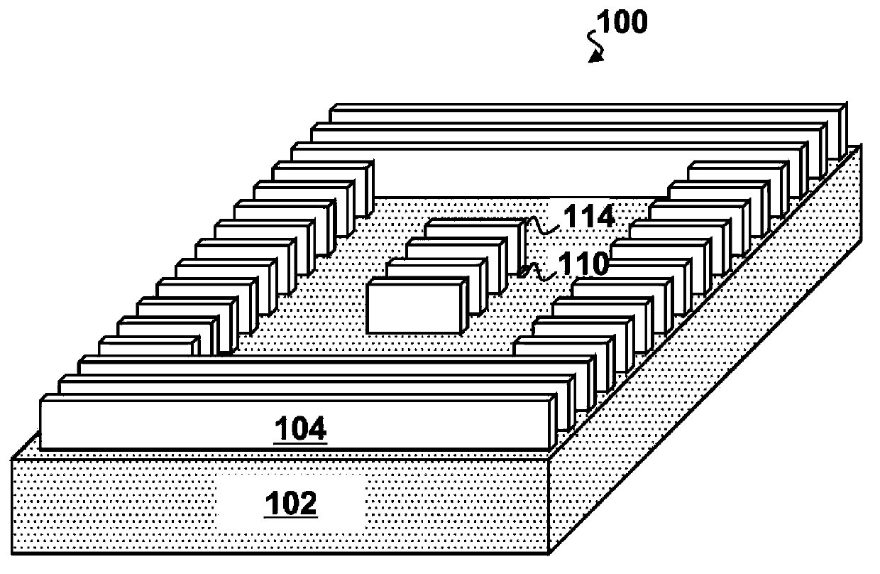
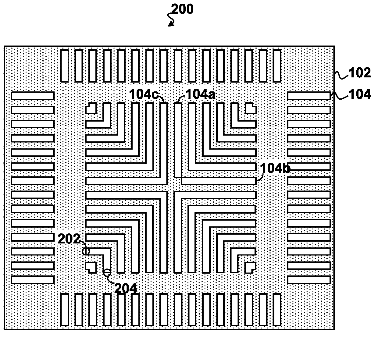
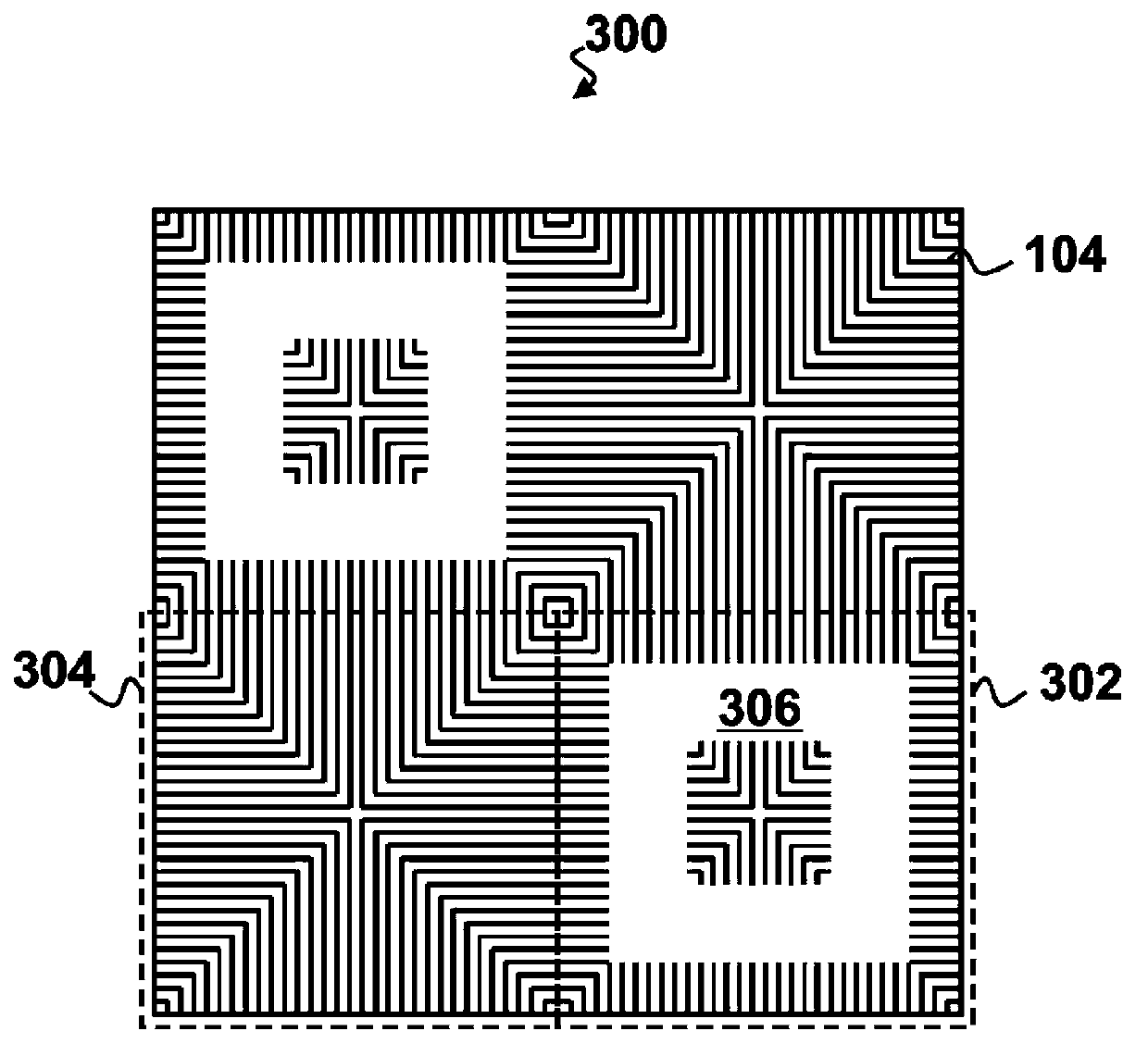
The invention discloses an overlay mark suitable for use in manufacturing nonplanar circuit devices and a method for forming the overlay mark are disclosed. An exemplary embodiment includes receiving a substrate having an active device region and an overlay region. One or more dielectric layers and a hard mask are formed on the substrate. The hard mask is patterned to form a hard mask layer feature configured to define an overlay mark fin. Spacers are formed on the patterned hard mask layer. The spacers further define the overlay mark fin and an active device fin. The overlay mark fin is cut to form a fin line-end used to define a reference location for overlay metrology. The dielectric layers and the substrate are etched to further define the overlay mark fin. The invention also provides the enhanced FINFET process overlay mark.

Description

technical field [0001] The present invention generally relates to the technical field of semiconductors, and more specifically, relates to an integrated circuit device and a method for forming the same. Background technique [0002] As the semiconductor industry has advanced to nanotechnology process nodes in the pursuit of higher device density, higher performance, and lower cost, challenges from manufacturing and design issues have resulted in three-dimensional devices such as Fin Field Effect Transistors (FinFETs) Design development. A typical FinFET is fabricated with thin "fins" extending from the substrate (eg, etched into the silicon layer of the substrate). The channel of the FET is formed in the vertical fin. A gate is disposed over (eg, wrapping) the fin. It is advantageous to have gates on both sides of the channel, allowing the gates to control the channel from both sides. Advantages of FinFET devices include reduced short-channel effects and higher current f...

Claims


Application Information

Patent Timeline
Patent Type & Authority Applications(China)
IPC IPC(8): H01L23/544
CPCG03F7/70633G03F7/70683H01L2924/0002H01L2924/00H01L23/544H01L27/0886H01L2223/54426H01L27/0883
Inventor 谢启文张岐康刘家助陈孟伟陈桂顺
Owner TAIWAN SEMICON MFG CO LTD
Learn More