3D IC and 3D CIS structure
A technology of integrated circuits and sensors, applied in the field of 3D integrated circuits and 3D image sensor structures, can solve problems such as FET performance impact
- Summary
- Abstract
- Description
- Claims
- Application Information
AI Technical Summary
Problems solved by technology
Method used
Image

Examples
Embodiment Construction
[0041] The making and using of various preferred embodiments of the invention are discussed in detail below. The present invention, however, provides many applicable concepts that can be implemented in a wide variety of specific contexts. The specific embodiments discussed are merely illustrative of specific ways to make and use the invention, and do not limit the scope of the invention.
[0042] The invention will be described with reference to preferred embodiments in a specific context, namely a three-dimensional (3D) integrated circuit or a 3D complementary metal-oxide-semiconductor (CMOS) image sensor (CIS). However, the concepts in the present invention are also applicable to other integrated circuits or semiconductor devices.
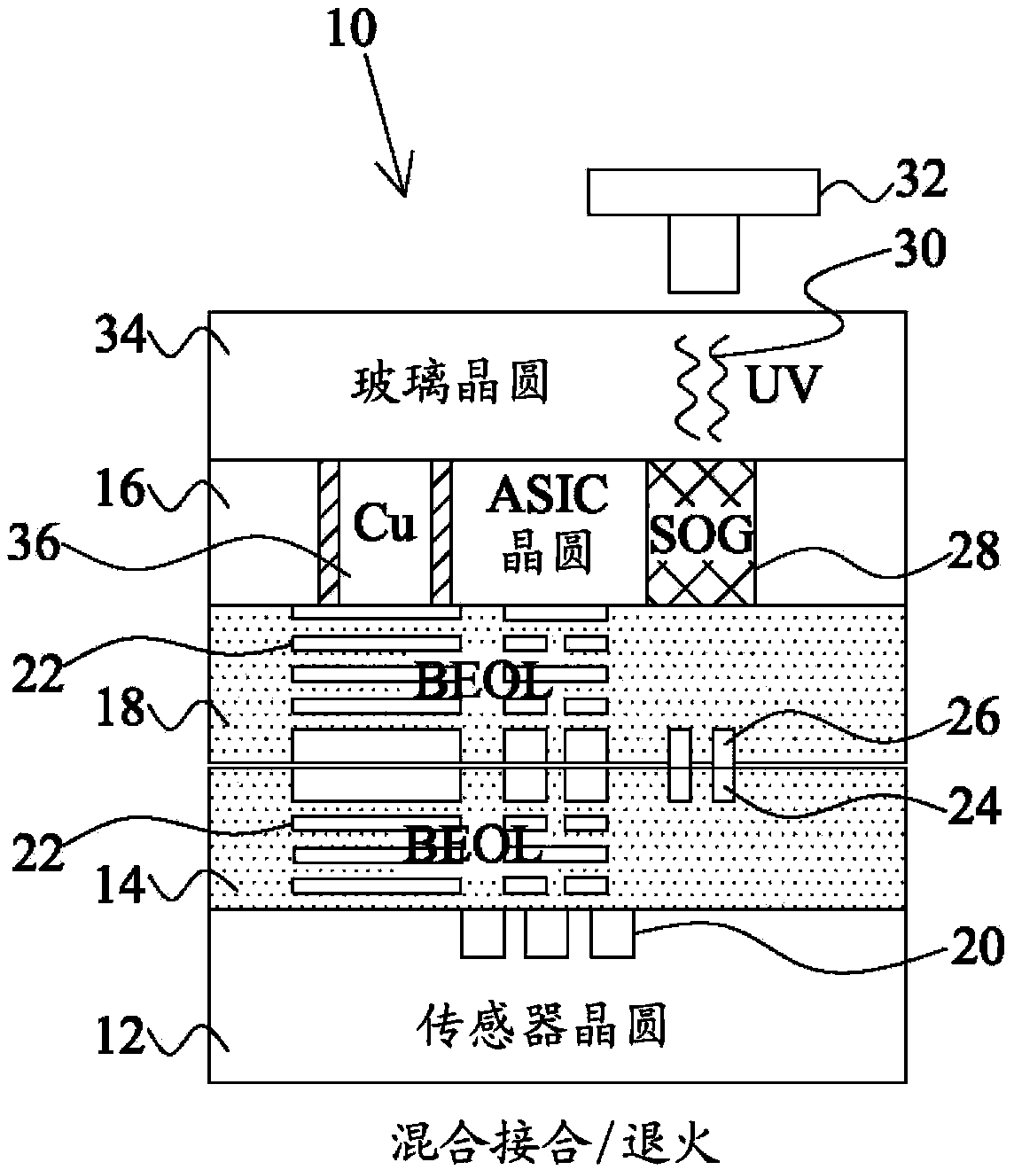
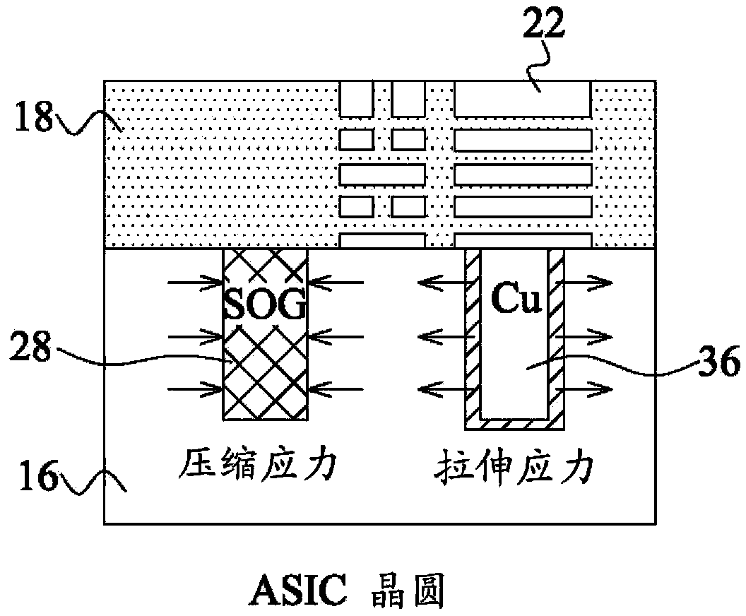
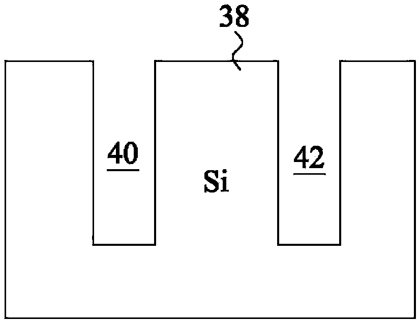
[0043] now refer to figure 1 , an embodiment of integrated circuit 10 is shown. The integrated circuit 10 includes a first wafer 12 , a first back end of line layer 14 , a second wafer 16 and a second back end of line layer 18 . In an embodi...
PUM
 Abstract
Description
Claims
Application Information
 - R&D
- Intellectual Property
- Life Sciences
- Materials
- Tech Scout
- Unparalleled Data Quality
- Higher Quality Content
- 60% Fewer Hallucinations
Browse by: Latest US Patents, China's latest patents, Technical Efficacy Thesaurus, Application Domain, Technology Topic, Popular Technical Reports.
© 2025 PatSnap. All rights reserved.Legal|Privacy policy|Modern Slavery Act Transparency Statement|Sitemap|About US| Contact US: help@patsnap.com