Organic electroluminescent display device and manufacturing method and display device thereof

An electroluminescence and device technology, applied in the manufacturing of organic semiconductor devices, electric solid-state devices, semiconductor/solid-state devices, etc., can solve the problems of cumbersome process, high cost, difficult curling, etc., to simplify the production process and avoid thickening. , The effect of good water and oxygen resistance

Inactive Publication Date: 2014-03-26
BOE TECH GRP CO LTD
View PDF16 Cites 11 Cited by
  • Summary
  • Abstract
  • Description
  • Claims
  • Application Information

AI Technical Summary

Problems solved by technology

[0006] In view of this, an embodiment of the present invention provides an organic electroluminescent display device, its preparation method and a display device, which are used to solve the cumbersome process and cost increase caused by the need for secondary film attachment of the existing organic electroluminescent display device. Problems with height and curly difficulty

Method used


Image

  • Organic electroluminescent display device and manufacturing method and display device thereof
  • Organic electroluminescent display device and manufacturing method and display device thereof
  • Organic electroluminescent display device and manufacturing method and display device thereof

Examples


example 1

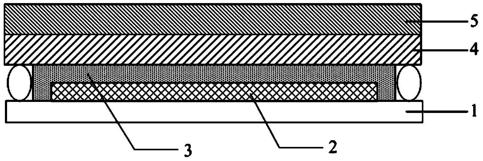
[0053] Example 1: Preparation by roll-to-roll method Figure 2a The substrate substrate shown, the schematic diagram of the specific process is shown in Figure 3a shown.

[0054] First, after the polarizing functional film layer 104 has undergone soaking and stretching processes, it is bonded to the main material film layer 101 and the first retardation film layer 102 on both sides of the polarizing functional film layer 104 in a roll-to-roll manner;

[0055] Afterwards, a water-blocking oxygen film layer 103 is deposited on one side of the first retardation film layer 102 to form the base substrate 100;

[0056] Finally, the organic electroluminescent pixel array 200 is fabricated on the base substrate 100 by using the existing process, and the organic electroluminescent pixel array 200 is packaged.

example 2

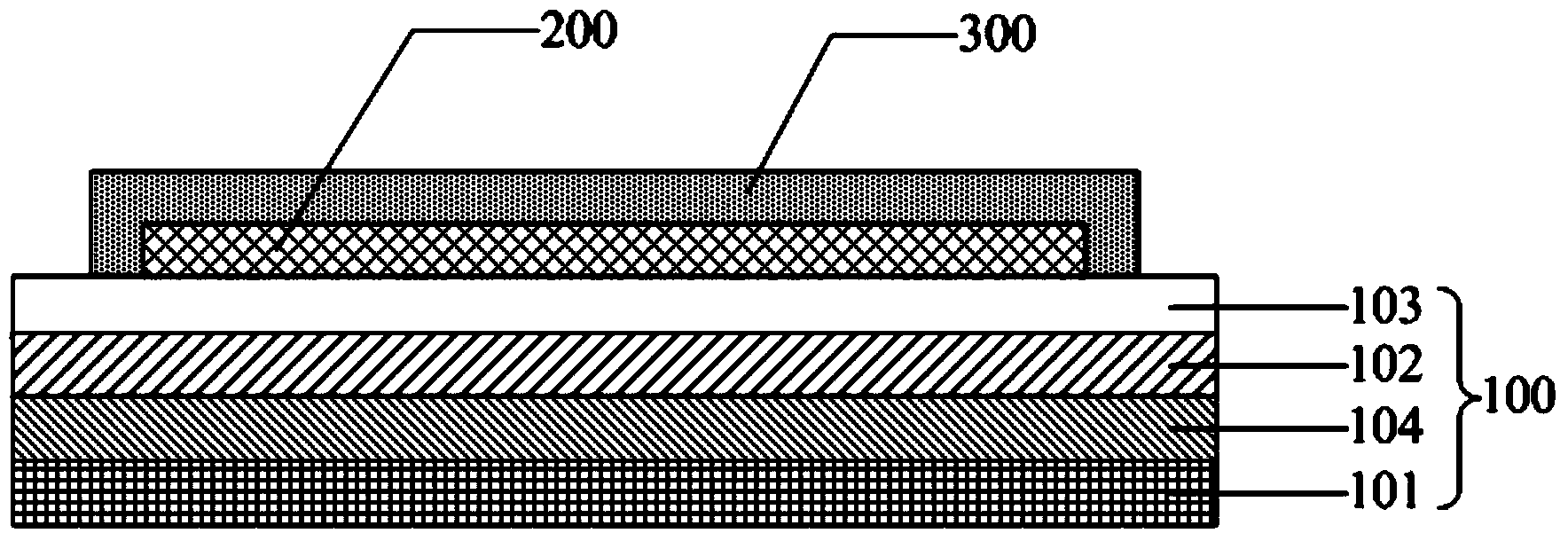
[0057] Example 2: Preparation by roll-to-roll method Figure 2b The substrate substrate shown, the schematic diagram of the specific process is shown in Figure 3b shown.

[0058] First, the polarizing functional film layer 104 is bonded to the main material film layer 101 in a roll-to-roll manner after soaking and stretching processes;

[0059] Afterwards, a water-blocking oxygen film layer 103 is deposited on one side of the polarizing functional film layer 104;

[0060] Then, the side where the water and oxygen blocking film layer 103 is deposited is laminated with the first retardation film layer 102 in a roll-to-roll manner to form the base substrate 100;

[0061] Finally, the organic electroluminescent pixel array 200 is fabricated on the base substrate 100 by using the existing process, and the organic electroluminescent pixel array 200 is packaged.

example 3

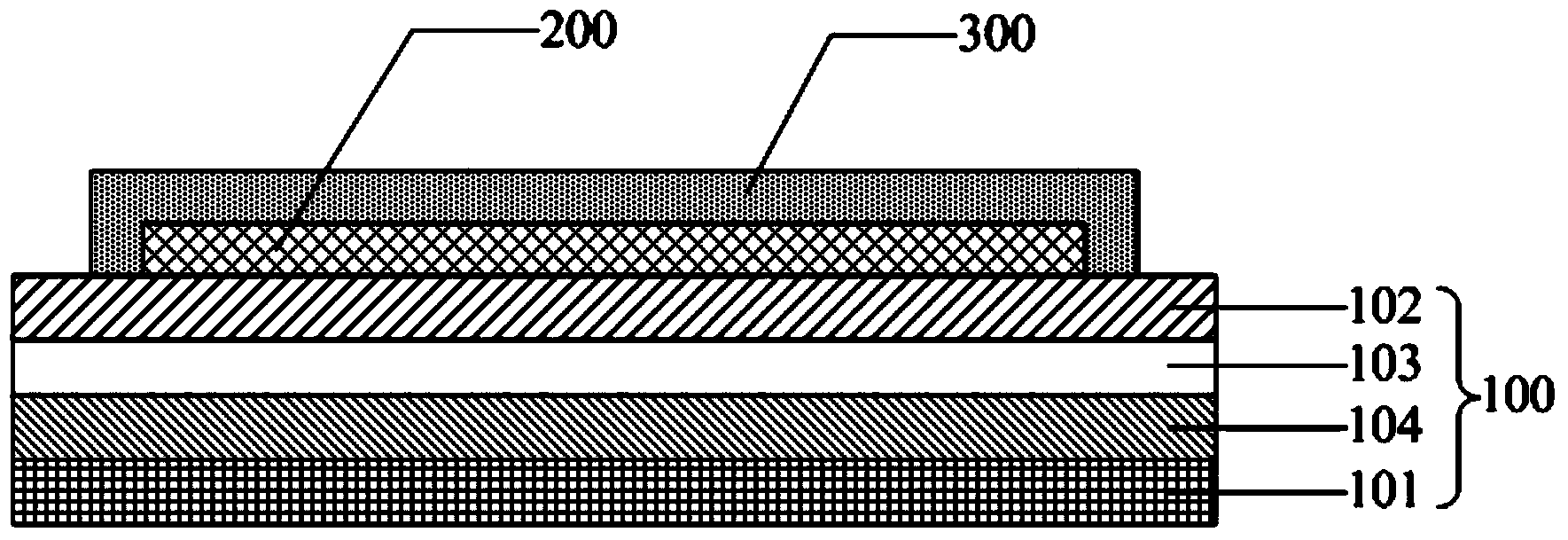
[0062] Example 3: Preparation by roll-to-roll method Figure 2c The substrate substrate shown, the schematic diagram of the specific process is shown in Figure 3c shown.

[0063] Firstly, after the polarizing functional film layer 104 has undergone soaking and stretching processes, it is bonded to the main material film layer 101 and the second retardation film layer 105 on both sides of the polarizing functional film layer 104 in a roll-to-roll manner;

[0064] Afterwards, a water-blocking oxygen film layer 103 is deposited on one side of the second retardation film layer 105;

[0065] Then, the side where the water and oxygen blocking film layer 103 is deposited is laminated with the first phase difference film layer 104 in a roll-to-roll manner to form the base substrate 100;

[0066] Finally, the organic electroluminescent pixel array 200 is fabricated on the base substrate 100 by using the existing process, and the organic electroluminescent pixel array 200 is packaged...


PUM


Abstract

The invention discloses an organic electroluminescent display device and a manufacturing method and a display device of the organic electroluminescent display device. A multifunctional composite film layer is adopted for a substrate bearing an organic electroluminescent pixel array. The substrate comprises a body material film layer, a first phase difference film layer, a water blocking oxygen film layer and a polarized light function film layer, wherein the body material film layer, the first phase difference film layer, the water blocking oxygen film layer and the polarized light function film layer are arranged in a mutual stacking mode, the first phase difference film layer and the polarized light function film layer have the anti-reflection effect after being combined, and the water blocking oxygen film layer has the water blocking oxygen performance. Thus, the substrate can have both the anti-reflection effect and the good water blocking oxygen performance, the secondary film pasting technology for pasting circular polarizers and the water blocking oxygen film layer on the bottom-emission type organic electroluminescent display device manufactured on the substrate can be omitted, the manufacturing process is simplified, production cost is reduced, and meanwhile the curving difficulty problem caused by the situation that the flexible device is thickened because of secondary film pasting can be avoided.

Description

technical field [0001] The invention relates to the field of display technology, in particular to an organic electroluminescence display device, a preparation method thereof and a display device. Background technique [0002] At present, compared with traditional liquid crystal display devices (Liquid Crystal Display, LCD), organic electroluminescent display devices (Organic Electroluminescent Display, OLED) have the characteristics of fast response, wide color gamut, ultra-thin, and flexibility. Has gradually become the mainstream of the display field. [0003] The structure of the OLED display device mainly includes: a base substrate, an organic electroluminescent pixel array fabricated on the substrate substrate; wherein, each organic electroluminescent pixel array includes an anode and a cathode arranged oppositely, and between the luminous layers. The light emission of the OLED display device is realized by exciting the organic material in the light-emitting layer to ...

Claims


Application Information

Patent Timeline
Patent Type & Authority Applications(China)
IPC IPC(8): H01L51/52H01L51/54H01L51/56
CPCH10K59/10H10K50/844H10K50/86H10K71/00Y02E10/549Y02P70/50H10K77/111H10K50/868H10K50/85H10K71/10H10K85/10H10K85/111H10K85/141H10K85/221H10K2102/00
Inventor 刘飞何璇曾庆慧谢明哲
Owner BOE TECH GRP CO LTD
Why Eureka
Try Eureka