Thin film packaging structure and organic photoelectric device

A technology for thin film packaging and optoelectronic devices, applied in the direction of electrical solid devices, electrical components, semiconductor devices, etc., can solve problems such as limited water and oxygen resistance, black spots, and extended edge water and oxygen erosion paths, so as to improve packaging performance and improve reliability effect

Active Publication Date: 2020-05-12
GUAN YEOLIGHT TECH CO LTD
View PDF7 Cites 0 Cited by
  • Summary
  • Abstract
  • Description
  • Claims
  • Application Information

AI Technical Summary

Problems solved by technology

However, there are currently two problems in thin film packaging. One is that the inorganic layer of thin film packaging has a certain stress. During use, the inorganic layer will peel off the cathode of the OLED screen from the organic layer of the OLED, resulting in black spots. When the OLED screen is cut by the cutter wheel, it will cause microcracks in the inorganic packaging layer, which will make the screen invalid. Since the inorganic barrier layer is very thin and belongs to the amorphous state, once the microcracks are formed, they will grow disorderly. This kind of crack growth belongs to Griffith The growth power of cracks comes from internal stress. There are two main ways to prevent such cracks. One is dam design to directly block the growth of micro-cracks. The other is to release its internal stress to prevent the growth of micro-cracks. At present, this kind of erosion is mainly slowed down by dame design. The design point of dame design is to design one or more rings of protrusions on the edge of the screen; and the height of the protrusions is below 5 μm, and its effect is only to extend the edge water. Oxygen attack path; its water and oxygen barrier properties are limited

Method used


Image

  • Thin film packaging structure and organic photoelectric device
  • Thin film packaging structure and organic photoelectric device
  • Thin film packaging structure and organic photoelectric device

Examples


Embodiment 1

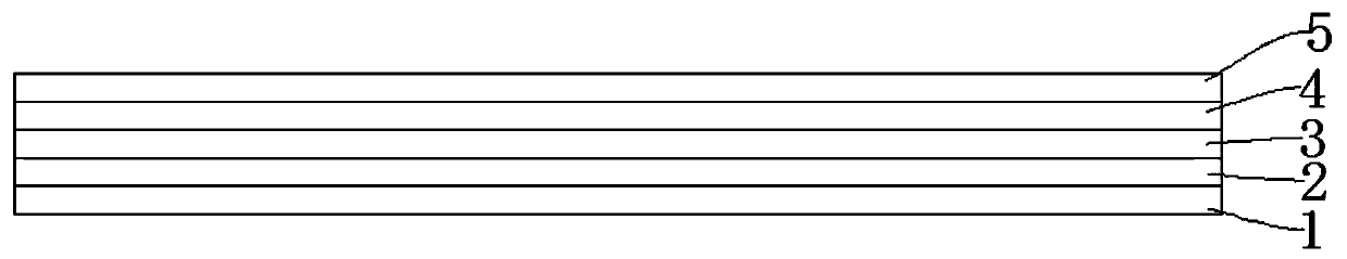
[0044] Such as figure 1 As shown, this embodiment provides a thin-film packaging structure, including a first inner packaging layer 1 , a metal layer 2 , a second inner packaging layer 3 , an adhesive layer 4 and an outer packaging layer 5 arranged sequentially from inside to outside. The first inner encapsulation layer 1 is an organic layer; the second inner encapsulation layer 3 is an inorganic layer or an organic-inorganic hybrid layer; the outer encapsulation layer 5 is a barrier film or a metal foil.

[0045] Wherein, the above "inner" refers to the side where the thin film packaging structure is in contact with the packaged device, and "outer" refers to the side of the thin film packaging structure away from the packaged device.

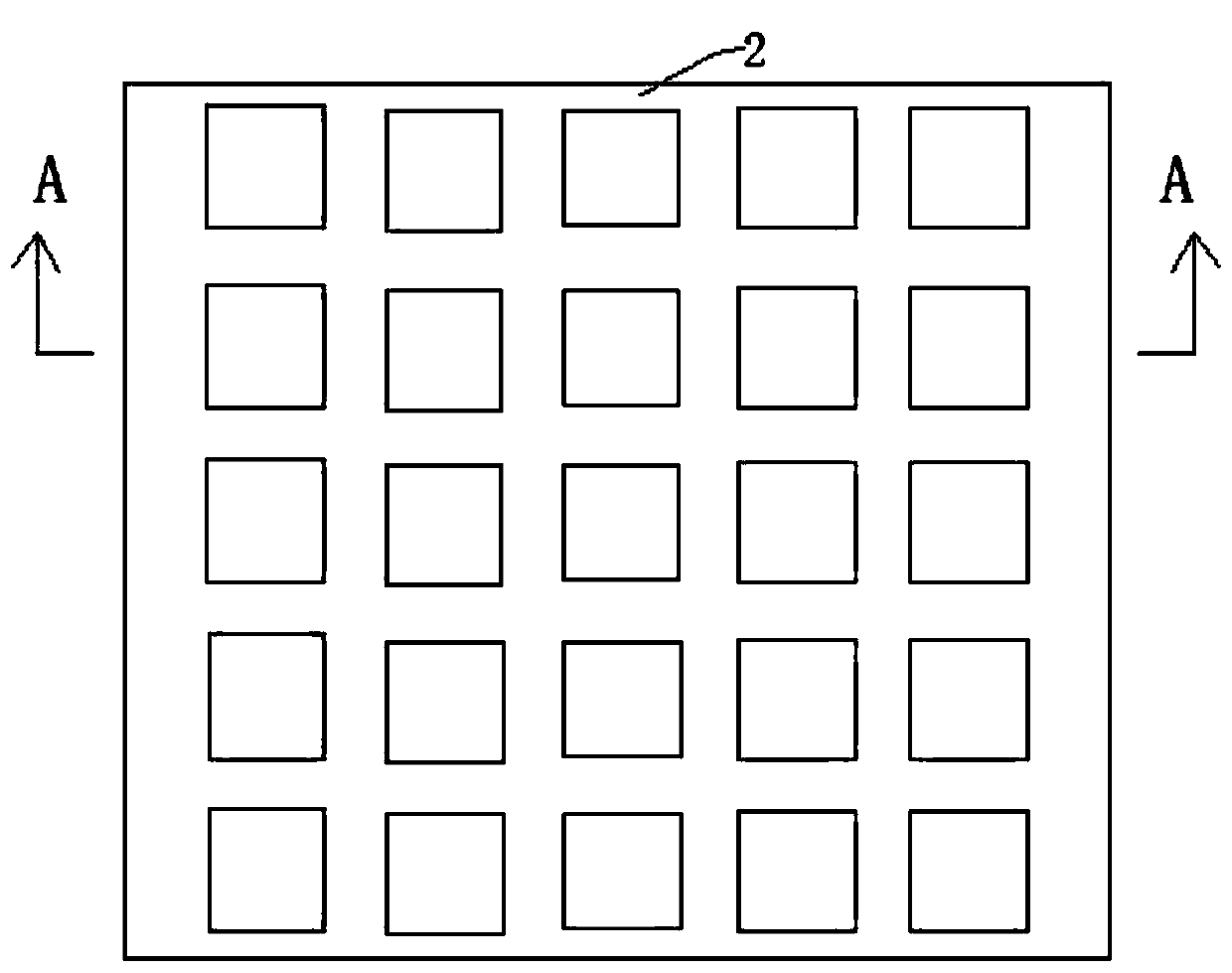
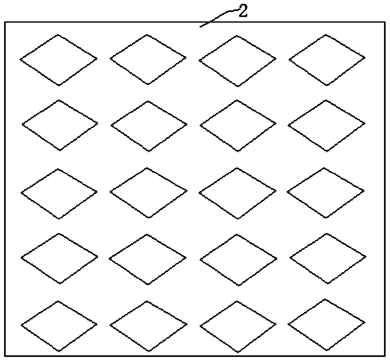
[0046]Wherein, the embodiment of the metal layer may optionally adopt any one of etching, mask, nanoimprinting, and laser transfer printing.

[0047] Wherein, the metal layer 2 may be implemented in the following ways:

[0048] 1. It can be a...

Embodiment 2

[0082] Such as Figure 13 and Figure 14 As shown, this embodiment provides an OLED device, which includes a substrate 6, a functional layer 7 sequentially arranged on the substrate 6, and a thin film encapsulation junction for encapsulating the functional layer 7 on the substrate 6, wherein the thin film encapsulation The structure adopts the implementation method in Example 1; the functional layer 7 includes a first electrode 8 , an organic functional layer 9 and a second electrode 10 .

[0083] in:

[0084] The substrate 6 can be a rigid substrate or a flexible substrate; the material of the first electrode 8 can be ITO (indium tin oxide), AZO (aluminum-doped zinc oxide), preferably ITO; the organic functional layer 9 includes a hole transport layer, a luminescent Layer and electron transport layer, provide light source for the whole device, prepared by evaporation, spin coating, inkjet printing, etc.; the second electrode 10 is used as a cathode, and the electrode materi...


PUM

PropertyMeasurementUnit
thicknessaaaaaaaaaa
thicknessaaaaaaaaaa
heightaaaaaaaaaa

Abstract

The invention provides a thin film packaging structure which is good in water-oxygen barrier property and can release inorganic layer stress to eliminate black spots and an organic photoelectric device using the thin film packaging structure. The thin film packaging structure comprises a first inner packaging layer, a metal layer, a second inner packaging layer, an adhesive layer and an outer packaging layer which are sequentially arranged from inside to outside. According to the invention, the above technical scheme is adopted, the metal layer is arranged between the first inner packaging layer and the second inner packaging layer of the thin film packaging structure, water and oxygen entering from the outside can form a compact metal oxide when encountering the metal layer, and the layerof oxide has a certain water and oxygen blocking performance, so that water and oxygen can be effectively prevented from entering the organic photoelectric device (such as an OLED device), the packaging performance of the organic photoelectric device is effectively improved, due to the arrangement of the metal layer, the stress of the second packaging layer can be released, and the situation thatblack spots appear on an OLED screen body due to electrode stripping of the second inner packaging layer is avoided.

Description

technical field [0001] The present application relates to the technical field of packaging of organic photoelectric devices, in particular to a thin film packaging structure and organic photoelectric devices. Background technique [0002] OLED is favored for its features such as bendable, foldable, thin and light, and high color saturation. As we all know, thin film encapsulation has excellent water and oxygen barrier properties and is widely used in OLED encapsulation. However, there are currently two problems in thin film packaging. One is that the inorganic layer of thin film packaging has a certain stress. During use, the inorganic layer will peel off the cathode of the OLED screen from the organic layer of the OLED, resulting in black spots. When the OLED screen is cut by the cutter wheel, it will cause microcracks in the inorganic packaging layer, which will make the screen invalid. Since the inorganic barrier layer is very thin and belongs to the amorphous state, onc...

Claims


Application Information

Patent Timeline
Patent Type & Authority Applications(China)
IPC IPC(8): H01L51/52
CPCH10K50/8426
Inventor 康建喜许显斌鲁天星王静朱映光
Owner GUAN YEOLIGHT TECH CO LTD
Why Eureka
Try Eureka