Method for drilling circuit board with high-precision and depth-controlled hole

A circuit board, high-precision technology, applied in the direction of electrical connection formation of printed components, etc., can solve the problems of uncontrolled, complex process control, unrealizable back drilling, etc., to eliminate differences in board thickness, ensure accuracy, and reduce distances. Effect

Inactive Publication Date: 2014-03-26
GUANGZHOU FASTPRINT CIRCUIT TECH +2
View PDF5 Cites 27 Cited by
  • Summary
  • Abstract
  • Description
  • Claims
  • Application Information

AI Technical Summary

Problems solved by technology

This method is greatly affected by the thickness of the dielectric layer. Usually, the thickness tolerance of the circuit board is 10%. That is to say, a 5mm thick circuit board can reach 1mm. Affected by glue flow during pressing, there is usually a deviation in the thickness between the center of the board and the board edge, and the board edge is usually thin, so back drilling or controlled depth drilling often results in

Method used


Image

  • Method for drilling circuit board with high-precision and depth-controlled hole
  • Method for drilling circuit board with high-precision and depth-controlled hole
  • Method for drilling circuit board with high-precision and depth-controlled hole

Examples


Embodiment 1

[0043] A method for high-precision depth-controlled drilling of circuit boards, including material cutting, inner-layer graphic production, etching, pressing, drilling, conductive hole production, conductive hole metallization, rimming, controlled-depth drilling, and outer-layer graphic production , surface treatment process; where:

[0044] Cutting, inner layer graphic making, pressing, outer layer graphic making, and surface treatment are carried out in accordance with conventional processes.

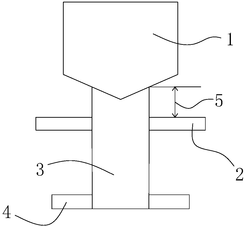
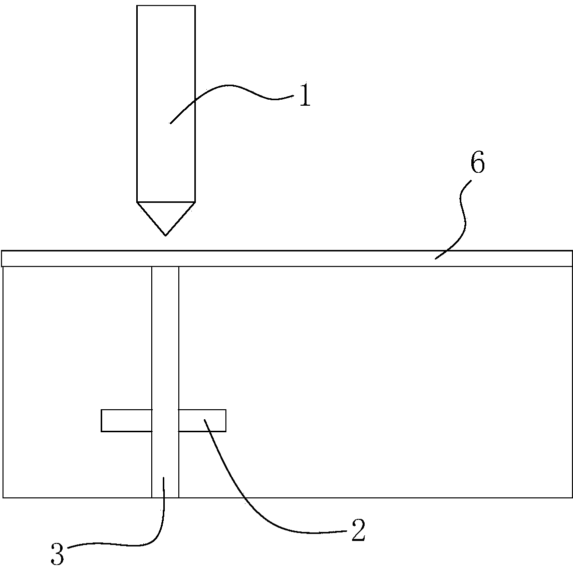
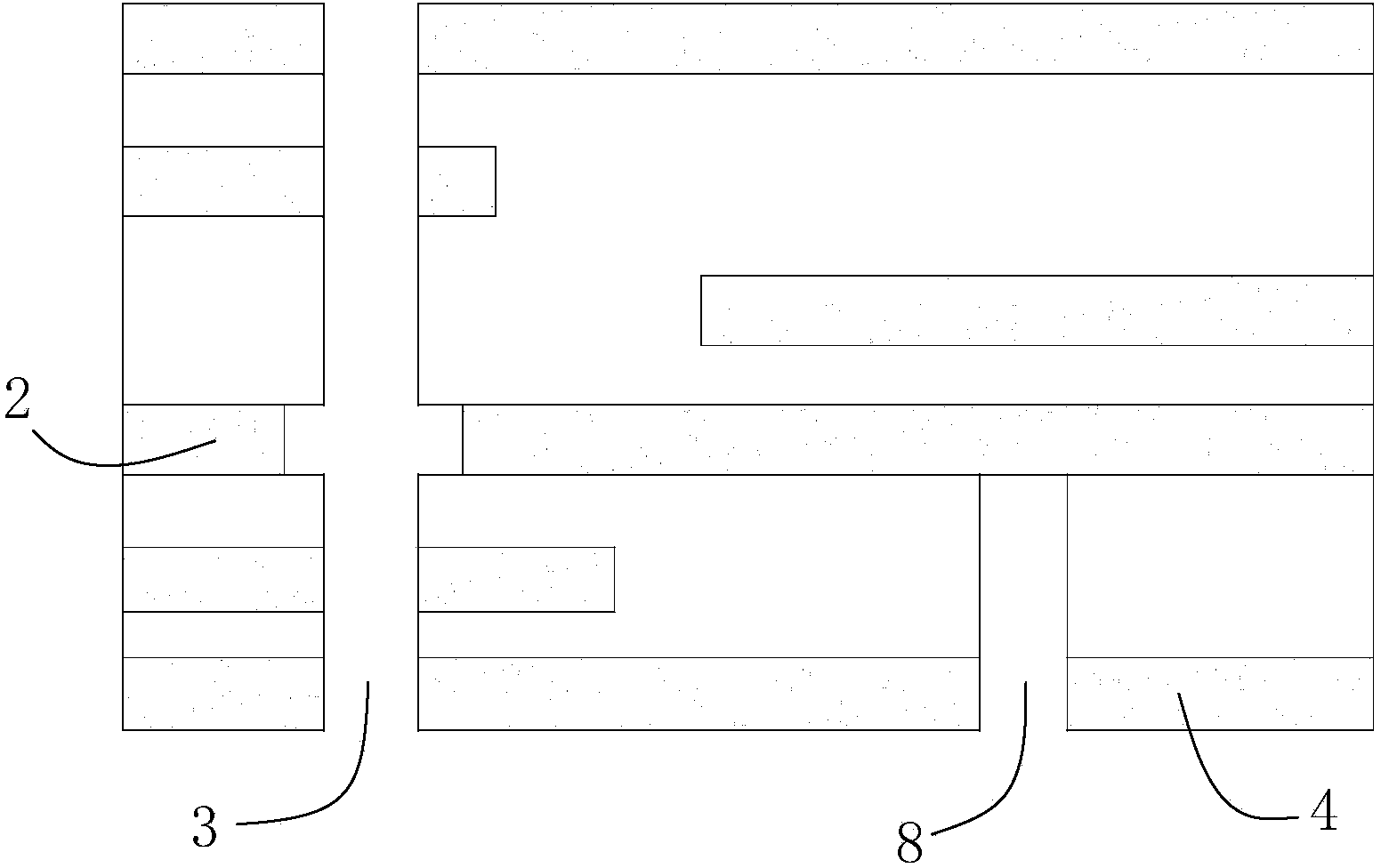
[0045] In the etching process, the positioning layer 7 is etched according to the predetermined design. In this embodiment, since the aperture of the depth control drill is designed to be 0.35mm, the conductive material at the wall of the hole drilled in the drilling process will be placed in the positioning layer. Etched away, the diameter of the etched area is 0.1mm larger than the aperture of the hole drilled in the drilling process; the positioning layer is insulated from the hole...

Embodiment 2

[0059] The method of the circuit board high-precision depth control drilling of this embodiment is basically the same as the method in embodiment 1, the difference is:

[0060] In the etching process, since the aperture of the depth control drill is designed to be 0.4 mm, the conductive material at the wall of the hole drilled in the positioning layer is etched away, and the diameter of the etching area is smaller than that of the hole drilled in the drilling process. The hole diameter is 0.1mm larger.

[0061] In the conductive hole metallization process, the conductive hole 8 and the through hole 3 drilled in the drilling process are metallized at the same time. Since the thickness-to-diameter ratio of the conductive hole is 1.2:1, copper (silver) paste is used to fill the hole. Metallize the inner wall of the conductive hole, make the positioning layer 7 conduct with the bottom surface 4 of the circuit board through the conductive hole 8, and insulate the through hole 3 fro...

Embodiment 3

[0065] The method of the circuit board high-precision depth control drilling of this embodiment is basically the same as the method in embodiment 1, the difference is:

[0066] In the etching process, since the aperture of the depth control drill is designed to be 0.45mm, the conductive material at the wall of the hole drilled in the positioning layer is etched away, and the diameter of the etched area is smaller than that of the hole drilled in the drilling process. The hole diameter is 0.15mm larger.

[0067] In the drilling process, the hole is drilled at the position where the depth needs to be controlled, and the drilling depth is to drill through the positioning layer to perform a high-precision depth-controlled blind hole process;

[0068] In the conductive hole manufacturing process, the conductive hole is drilled in the edge area of ​​the circuit board by using the method of deep-controlled drilling to process the blind hole.

[0069] In the conductive hole metalliza...


PUM

PropertyMeasurementUnit
Depthaaaaaaaaaa

Abstract

The invention discloses a method for drilling a circuit board with a high-precision and depth-controlled hole, and belongs to the technical field of printed circuit boards. The method comprises the working procedures of inner layer image manufacturing, etching, pressing, drilling, electric conduction hole manufacturing, electric conduction hole metalizing, edge milling and depth-controlled drilling. Due to the fact that the electric conduction hole manufacturing is added, a positioning layer on a target layer is led out to the bottom face of the circuit board through an electric conduction blind hole, the positioning layer can serve as a signal induction layer, the distance from the signal induction layer to the target layer is reduced, and the purpose of eliminating the plate thickness difference is achieved. The high-precision and depth-controlled drilling can be carried out. The method is suitable for widely manufacturing high-precision back drilling and depth-controlled blind holes.

Description

technical field [0001] The invention relates to a manufacturing process method of a printed circuit board, in particular to a method for drilling a circuit board with high-precision depth control. Background technique [0002] In the field of printed circuit board technology, with the expansion of the business of switching, transmission, wireless and data communication telecommunication products and the improvement of technology, many complex systems are more dependent on the connections, wiring, and plugging on the backplane connectors to handle high-speed data streams. In order to reduce signal loss and interference, back-drilling technology is used in PCB design, and the precision requirements are getting higher and higher. In some designs, the length of residual copper above the target layer is required, such as figure 1 The shown stub5 length is 0.1mm or even shorter is required. In the general back-drilling process, it is firstly required that the target layer (ie, th...

Claims


Application Information

Patent Timeline
IPC IPC(8): H05K3/40H05K3/42
Inventor 陈曦刘攀曾志军
Owner GUANGZHOU FASTPRINT CIRCUIT TECH
Why Eureka
Try Eureka