Array substrate, preparation method thereof and display device

A technology for array substrates and display devices, which is applied in the manufacture of semiconductor/solid-state devices, electrical components, diodes, etc., can solve the problems of complex structure, reduce the production yield of array substrates, and difficult to prepare high array substrates, so as to ensure production safety and The effect of production efficiency

Active Publication Date: 2014-04-02
BOE TECH GRP CO LTD
View PDF5 Cites 22 Cited by
  • Summary
  • Abstract
  • Description
  • Claims
  • Application Information

AI Technical Summary

Problems solved by technology

[0003] In the process of realizing the OLED array substrate, the inventor found that in order to prevent disconnection and defects when forming the OLED electrodes on the color film, the conventional technology needs to set a flat protective layer between the OLED electrodes and the color film, but this structure is relatively complicated Increased the difficulty of preparing the array substrate and reduced the production yield of the array substrate

Method used


Image

  • Array substrate, preparation method thereof and display device
  • Array substrate, preparation method thereof and display device
  • Array substrate, preparation method thereof and display device

Examples


Embodiment 1

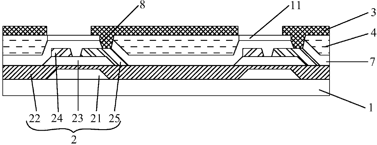
[0058] An embodiment of the present invention provides an array substrate, such as figure 1As shown, it includes a base substrate 1, a thin film transistor unit 2 located on the base substrate 1, a color filter 4 and a flat protective layer 3, and the flat protective layer 3 is connected to the drain 25 of the thin film transistor unit 2 electrical connection, wherein the flat protective layer 3 is conductive.

[0059] Wherein, the flat protective layer 3 formed on the array substrate is usually formed by a resin with a certain viscosity, which can flatten the uneven structure on the array substrate, and protect the structure under the flat protective layer 3 from being damaged. Corrosion, to ensure that the subsequent manufacturing process of the array substrate can be carried out smoothly.

[0060] But in the embodiment of the present invention, the flat protective layer 3 can also conduct electricity, so that the flat protective layer 3 can not only play the role of flat p...

Embodiment 2

[0106] The embodiment of the present invention provides a method for preparing the array substrate described in Embodiment 1, such as Figure 10 Shown, this preparation method comprises:

[0107] Step S101 , forming a pattern including a drain of a thin film transistor unit, a color filter and a flat protection layer electrically connected to the drain of the thin film transistor unit.

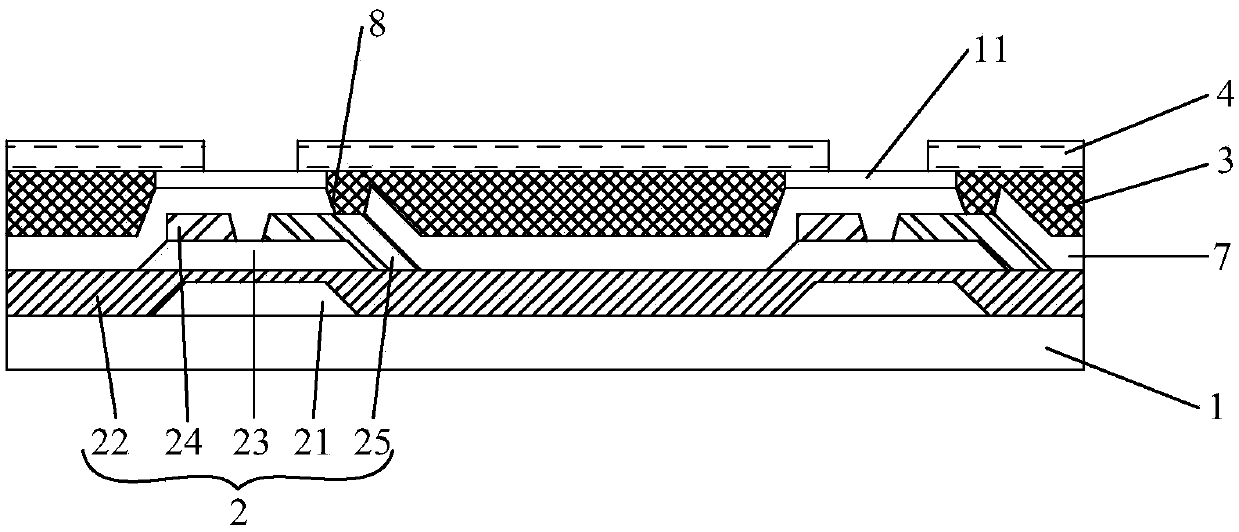
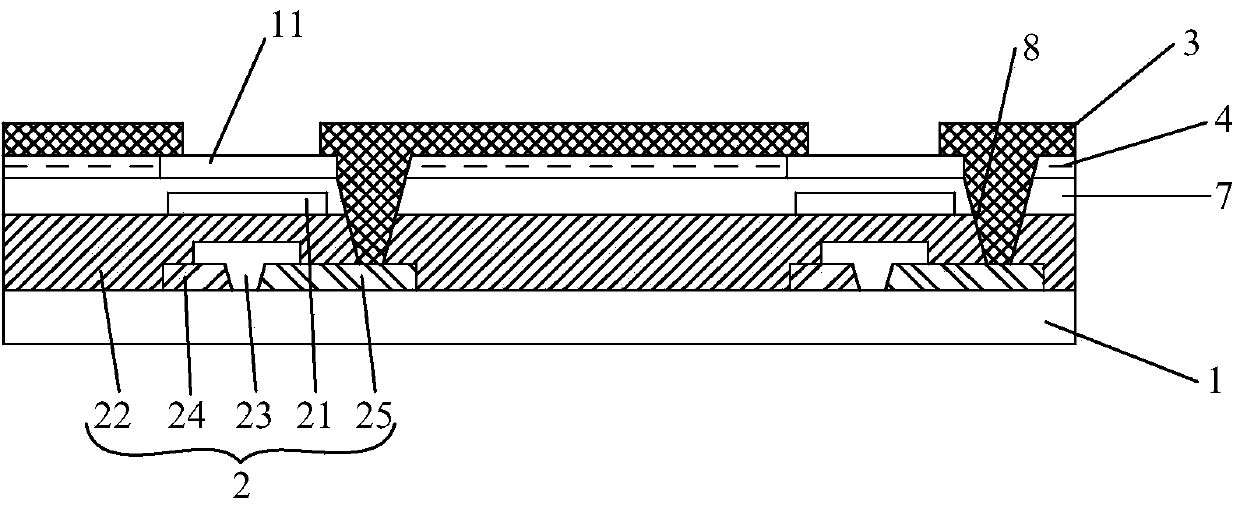
[0108] Thus, it is possible to form Figure 1-Figure 7 The shown flat protective layer 3 is electrically connected to the array substrate with the drain electrode 25 . Specifically, it can be known from Embodiment 1 that the array substrate provided by the embodiment of the present invention is at least as Figure 1-7 In the seven structures shown, that is, the drain 25 of the thin film transistor unit 2 can be either above the flat protective layer 3 or below the flat protective layer 3, and the thin film transistor unit 2 can be a bottom gate type Also available as top gate type.

[0109...


PUM

PropertyMeasurementUnit
sizeaaaaaaaaaa

Abstract

The embodiment of the invention discloses an array substrate, a preparation method thereof and a display device, and relates to the technical field of display. According to the array substrate, the preparation method and the display device, disclosed by the invention, the layer structure of the array substrate can be simplified, the preparation difficulty of the array substrate can be reduced, and thus the production yield of the array substrate can be increased. The array substrate comprises a liner substrate, a TFT (Thin Film Transistor) unit, a colorful film and a flat protection layer, wherein the TFT unit is positioned above the liner substrate, the flat protection layer is electrically connected with a drain electrode of the TFT unit, and the flat protection layer is conductive.

Description

technical field [0001] The present invention relates to the field of display technology, in particular to an array substrate, a preparation method thereof, and a display device. Background technique [0002] Organic Light Emitting Diode (OLED) is an organic thin-film electroluminescent device, which has the advantages of simple preparation process, low cost, high luminous efficiency, easy formation of flexible structure, and wide viewing angle; therefore, the use of organic light emitting Diode display technology has become an important display technology. [0003] In the process of realizing the OLED array substrate, the inventor found that in order to prevent disconnection and defects when forming the OLED electrodes on the color film, the conventional technology needs to set a flat protective layer between the OLED electrodes and the color film, but this structure is relatively complicated The difficulty of preparing the array substrate is increased, and the production y...

Claims


Application Information

Patent Timeline
Patent Type & Authority Applications(China)
IPC IPC(8): H01L27/12H01L27/32H01L21/77
CPCH01L27/124H10K59/38H10K59/123H10K59/126H10K50/813H10K50/81H10K50/865H10K50/844H10K59/122H10K71/00H10K59/1201
Inventor 齐永莲舒适赵明
Owner BOE TECH GRP CO LTD
Why Eureka
Try Eureka