
Data processing method and device

A data processing and data technology, applied in the direction of input/output to record carrier, signal generation/distribution, memory address/allocation/relocation, etc., can solve problems such as insufficient timing margin and inability to collect correctly. The effect of acquisition and ensuring timing margin

Active Publication Date: 2016-08-17
LOONGSON TECH CORP
View PDF4 Cites 0 Cited by
  • Summary
  • Abstract
  • Description
  • Claims
  • Application Information

AI Technical Summary

Problems solved by technology

[0004] Embodiments of the present invention provide a data processing method and device to at least solve the technical problem of inability to collect data correctly due to insufficient timing margin on the cross-clock domain transmission path when collecting memory read data

Method used


Image

  • Data processing method and device
  • Data processing method and device
  • Data processing method and device

Examples


Embodiment 1

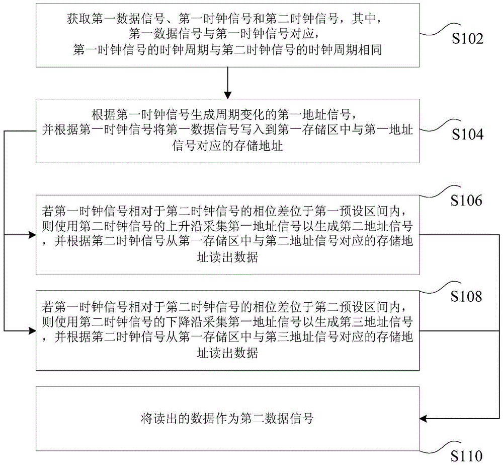
[0020] According to an embodiment of the present invention, a data processing method is provided, such as figure 1 As shown, the method includes:

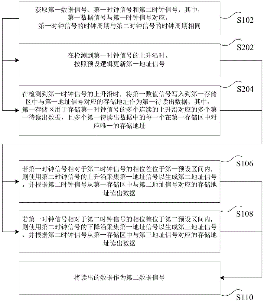
[0021] S102: Acquire a first data signal, a first clock signal, and a second clock signal, wherein the first data signal corresponds to the first clock signal, and the clock period of the first clock signal is the same as the clock period of the second clock signal;

[0022] S104: Generate a periodically changing first address signal according to the first clock signal, and write the first data signal into a storage address corresponding to the first address signal in the first storage area according to the first clock signal;

[0023] S106: If the phase difference between the first clock signal and the second clock signal is within the first preset interval, use the rising edge of the second clock signal to collect the first address signal to generate a second address signal, and The signal reads data from the storage address cor...

Embodiment 2

[0064] According to an embodiment of the present invention, a data processing method is also provided, such as Figure 6 As shown, the method includes:

[0065] S602: Obtain a system clock signal corresponding to the memory controller, obtain a read data signal and a read data strobe signal returned by each of the multiple memory chips, and delay the read data strobe signal;

[0066] S604: Process the read data signal corresponding to each of the plurality of memory chips according to the data processing method in Embodiment 1, and read out the signal from the first storage area, or the first storage area and the second storage area The data is used as the collected memory read data, wherein the first data signal is a read data signal, the first clock signal is a delayed read data strobe signal, and the second clock signal is a system clock signal;

[0067] S606: Synchronize the collected memory read data corresponding to each of the multiple memory chips, and send the synchr...

Embodiment 3

[0071] According to an embodiment of the present invention, a data processing device for implementing the above data processing method is also provided, such as Figure 7 As shown, the device includes:

[0072] 1) The first address generation circuit 702 includes a first trigger input terminal and a first address output terminal, wherein the first address generation circuit 702 is configured to generate an address according to a first clock signal input from the first trigger input terminal A first address signal that changes periodically, and outputs the first address signal from the first address output terminal;

[0073] 2) The second address generating circuit 704 includes a second trigger input terminal, a third trigger input terminal, a first address input terminal and a second address output terminal, the first address input terminal is directly or indirectly connected to the first address Output terminal, wherein, the second address generating circuit 704 is used to d...


PUM


Abstract

The invention discloses a data processing method and device. The method comprises the steps of generating a first address signal according to a first clock signal, and writing a first data signal in a memory address, corresponding to the first address signal, in a first memory area according to the first clock signal; if the phase difference, relative to a second clock signal, of the first clock signal is located in a first preset section, using the rising edge of the second clock signal for collecting the first address signal so as to generate a second address signal, and reading data from a memory address, corresponding to the second address signal, in the first memory area according to the second clock signal; if the phase difference is located in a second preset section, using the falling edge of the second clock signal for collecting the first address signal to generate a third address signal, and reading data from the memory address, corresponding to the third address signal, in the first memory area according to the second clock signal; using the read data as a second data signal. According to the data processing method and device, the problem caused by the insufficient timing sequence margin of a data clock domain crossing transmission path is solved.

Description

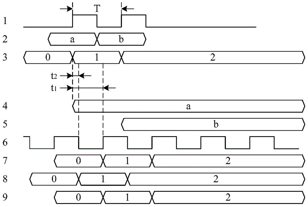
technical field [0001] The present invention relates to the field of sequential logic circuits, in particular to a data processing method and device. Background technique [0002] In the existing solutions for cross-clock domain transmission of data signals, the transition edge of one clock signal is usually used to collect the data signal corresponding to another clock signal, so as to obtain the data signal corresponding to the previous clock signal. However, in this scheme, the timing margin of the data signal on the transmission path transmitted across the clock domain is uncontrollable and uncertain, and its timing margin can be larger in one situation or larger in another. When the timing margin is small, because the duration of the updated value of the data signal as the acquisition object is relatively short, its data state is relatively unstable, so the collected data is not accurate, which affects the Reliability of transmission of data signals across clock domain...

Claims


Application Information

Patent Timeline
Patent Type & Authority Patents(China)
IPC IPC(8): G06F12/02G06F3/06G06F1/04
Inventor 黄帅王焕东陈新科
Owner LOONGSON TECH CORP
Learn More