2D/3D analysis for abnormal tools and stage diagnosis

An anomaly and tool technology, applied in the field of semiconductor processing systems, can solve problems such as difficult to determine abnormal tool and stage performance

Active Publication Date: 2014-04-09
TAIWAN SEMICON MFG CO LTD
View PDF2 Cites 4 Cited by
  • Summary
  • Abstract
  • Description
  • Claims
  • Application Information

AI Technical Summary

Problems solved by technology

Therefore, it is difficult to determine abnormal tool and

Method used


Image

  • 2D/3D analysis for abnormal tools and stage diagnosis
  • 2D/3D analysis for abnormal tools and stage diagnosis
  • 2D/3D analysis for abnormal tools and stage diagnosis

Examples


Embodiment Construction

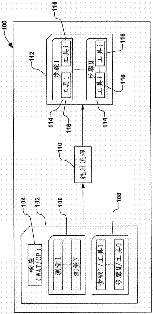
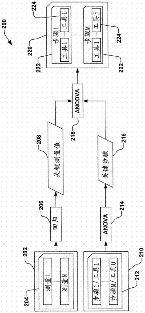
[0033] The present invention provides a multidimensional analysis flow to rank suspect tools and process steps in the absence of interference from other relevant factors or influences, such as processing in one step that may affect measurements in subsequent steps. Accordingly, the present invention provides a method of efficiently sequencing tools and process steps in the order of the anomalies demonstrated in each corresponding tool and process step.

[0034] Accordingly, the following description refers to the accompanying drawings, wherein like reference numerals are generally used to designate like elements throughout, the various drawings not necessarily being drawn to scale. In the following description, for purposes of explanation, numerous specific details are set forth to facilitate understanding. It will be understood, however, by those skilled in the art that one or more aspects described herein may be practiced with a lesser degree of these specific details. In o...


PUM


Abstract

A method for analyzing abnormalities in a semiconductor processing system includes performing an analysis of variance on a production history associated with each of a plurality of tools at each of a plurality of process steps for each of a plurality of processed wafers, and identifying key process steps. A regression analysis on a plurality of measurements of the plurality of wafers at each process step is performed and key measurement parameters are identified. An analysis of covariance on the key measurement parameters and key process steps, and the key process steps are ranked based on an f-ratio, therein ranking an abnormality of the key process steps. Further, the plurality of tools associated with each of the key process steps are ranked based on an orthogonal t-ratio associated with an analysis of covariance, therein ranking an abnormality each tool associated with the key process steps. The invention also provides 2D/3D analysis for abnormal tools and stage diagnosis.

Description

technical field [0001] The present invention relates generally to the field of semiconductor technology, and more particularly, to semiconductor processing systems. Background technique [0002] In semiconductor manufacturing, a semiconductor wafer typically goes through many process steps, or stages, before a complete die is formed. For example, such process steps may include photolithography, etching, semiconductor doping, and deposition of various materials on the semiconductor wafer. The accuracy and precision of the process and the transitions between different process steps often directly affect the quality of the complete die. For example, deviations in the gate structure, imprecise doping concentrations, or excessively thick or thin dielectric layers can create unwanted leakage currents in transistors or delays in circuit operation. [0003] Further complicating the challenge is the desire of semiconductor manufacturers to maximize the number of dies produced throu...

Claims


Application Information

Patent Timeline
IPC IPC(8): G06F17/50
CPCG06F17/50G03F7/70533G03F7/70616G05B23/024H01L22/00G06F30/00
Inventor 林俊贤陈瑞龙赵蕙韵牟忠一林进祥
Owner TAIWAN SEMICON MFG CO LTD
Why Eureka
Try Eureka