Array substrate, manufacturing method thereof and display device
What is Al technical title?
Al technical title is built by PatSnap Al team. It summarizes the technical point description of the patent document.
A technology of an array substrate and a manufacturing method, which is applied in the field of display, can solve problems such as the complexity of the manufacturing process of the array substrate, and achieve the effect of reducing manufacturing process steps and reducing manufacturing costs
Active Publication Date: 2014-04-09
BOE TECH GRP CO LTD
View PDF13 Cites 16 Cited by
Summary
Abstract
Description
Claims
Application Information
AI Technical Summary
This helps you quickly interpret patents by identifying the three key elements:
Problems solved by technology
Method used
Benefits of technology
Problems solved by technology
[0004] The technical problem to be solved by the present invention is the complicated manufacturing process of the existing array substrate
Method used
Image
Click on the blue label to locate the original text in one second.
Reading with bidirectional positioning of images and text.
Examples
Embodiment Construction
[0025] The embodiments of the present invention will be described in detail below in conjunction with the accompanying drawings.
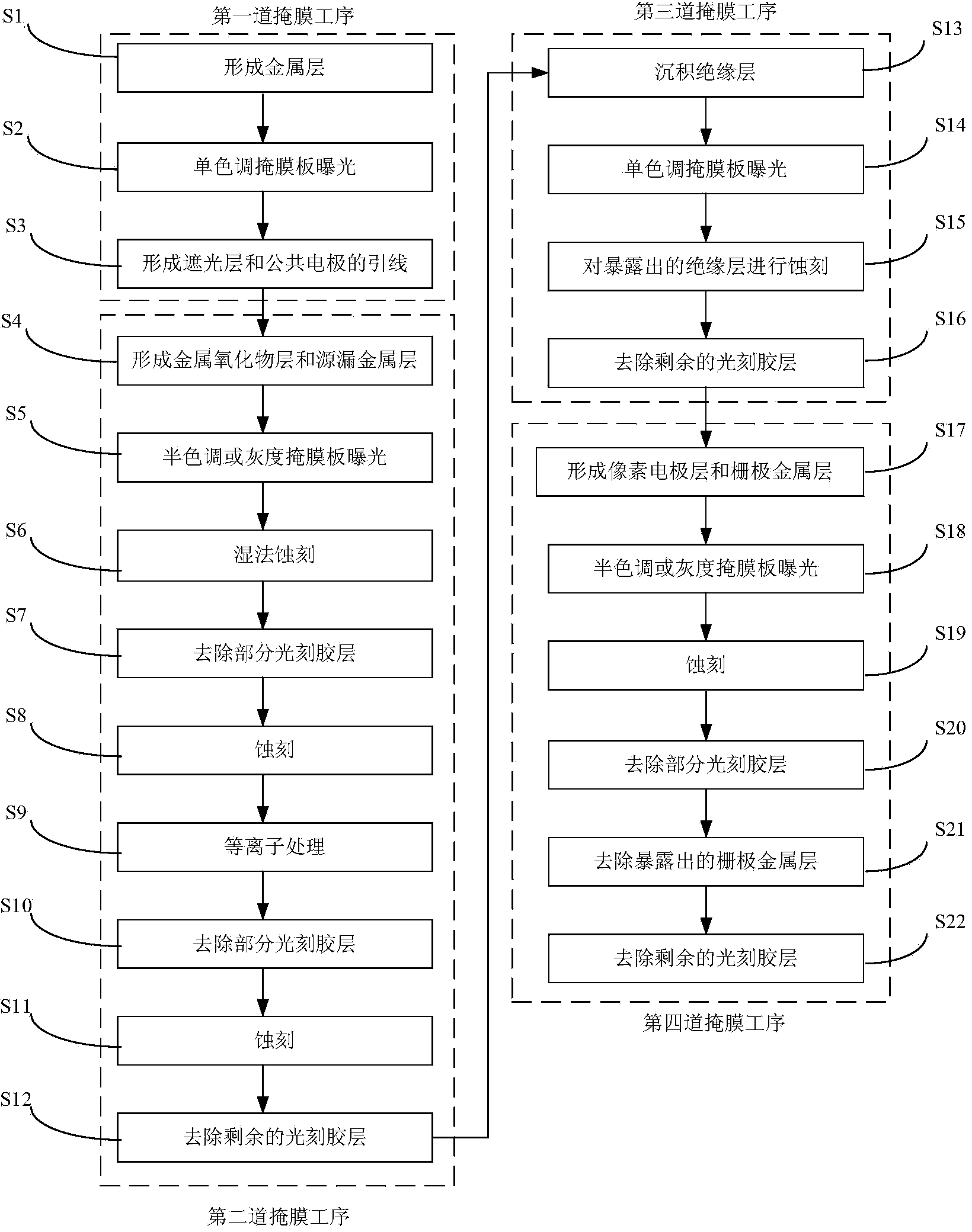
[0026] figure 1 A flowchart of a method for manufacturing an array substrate according to an embodiment of the present invention is shown. Such as figure 1 As shown, the manufacturing method of the array substrate according to the embodiment of the present invention uses a total of four masking processes, which is four fewer than the eight masking processes required for manufacturing ultra-advanced super-dimensional field conversion array substrates. The manufacturing process steps of the array substrate are reduced, and the manufacturing cost of the array substrate is reduced. The following will combine Figure 2 to 17 The manufacturing method of the array substrate according to the embodiment of the present invention will be described in detail.
[0027] First, introduce the first mask process.
[0028] Step S1: Deposit a metal layer on the substrate...
PUM
Abstract
The invention relates to an array substrate, a manufacturing method of the array substrate and a display device. The manufacturing method of the array substrate is characterized in that a source electrode, a drain electrode, an active layer and a first transparent electrode of a thin film transistor in the array substrate are formed through a masking work procedure, the active layer and the first transparent electrode are formed by the same metal oxide layer, the source electrode and the drain electrode are located above the active layer, the first transparent electrode corresponds to a first semi-light-transmitting region of a mask plate, a channel region of the thin film transistor corresponds to a second semi-light-transmitting region of the mask plate, the source electrode and the drain electrode of the thin film transistor correspond to the non-light-transmitting region of the mask plate, and the light transmittance of the first semi-light-transmitting region of the mask plate is larger than the light transmittance of the second semi-light-transmitting region of the mask plate.
Description
Technical field [0001] The present invention relates to the field of display technology, in particular to an array substrate, a manufacturing method thereof, and a display device. Background technique [0002] Liquid crystal display devices are widely used in televisions, monitors, notebook computers, tablet computers and other equipment due to their small size, low power consumption, and low radiation. [0003] At present, in the manufacture of HADS (High Advanced Dimension Switch) type array substrates, eight masking processes are usually required, which are followed by the gate electrode, the gate insulating layer, the etching stop layer, and the source-drain metal layer. , The passivation layer, the common electrode, the passivation layer and the pixel electrode are patterned. As for each masking process, a costly mask needs to be manufactured, and process steps such as exposure, development, etching, and ashing need to be performed, which makes the existing array substrate ma...
Claims
Application Information
Patent Timeline
Application Date:The date an application was filed.
Publication Date:The date a patent or application was officially published.
First Publication Date:The earliest publication date of a patent with the same application number.
Issue Date:Publication date of the patent grant document.
PCT Entry Date:The Entry date of PCT National Phase.
Estimated Expiry Date:The statutory expiry date of a patent right according to the Patent Law, and it is the longest term of protection that the patent right can achieve without the termination of the patent right due to other reasons(Term extension factor has been taken into account ).
Invalid Date:Actual expiry date is based on effective date or publication date of legal transaction data of invalid patent.