3-D single floating gate non-volatile memory device

一种非易失性、存储器的技术,应用在半导体器件、电固体器件、电气元件等方向,达到缩短工艺工时、降低成本、保证良率的效果

Active Publication Date: 2014-04-09
XINLIJIA INTEGRATED CIRCUIT (HANGZHOU) CO LTD
View PDF5 Cites 8 Cited by
  • Summary
  • Abstract
  • Description
  • Claims
  • Application Information

AI Technical Summary

Problems solved by technology

[0005] On the other hand, in terms of shrinking semiconductor NVM devices smaller than the 20nm process technology generation, due to the limitations of lithographic and etching processes, such as double-gate alignment and stacked double-gate processes The ultra-high (ultra-high) anisotropic (an-isotropic) etch aspect ratio (aspect ratio), the traditional semiconductor NVM device is also encountering the obstacle of the floating gate NVM device

Method used


Image

  • 3-D single floating gate non-volatile memory device
  • 3-D single floating gate non-volatile memory device
  • 3-D single floating gate non-volatile memory device

Examples


Embodiment Construction

[0028] The following description will enumerate a plurality of preferred exemplary embodiments of the present invention, those familiar with the art should understand that the present invention can be implemented in various possible ways, and are not limited to the following exemplary embodiments or those in the embodiments feature.

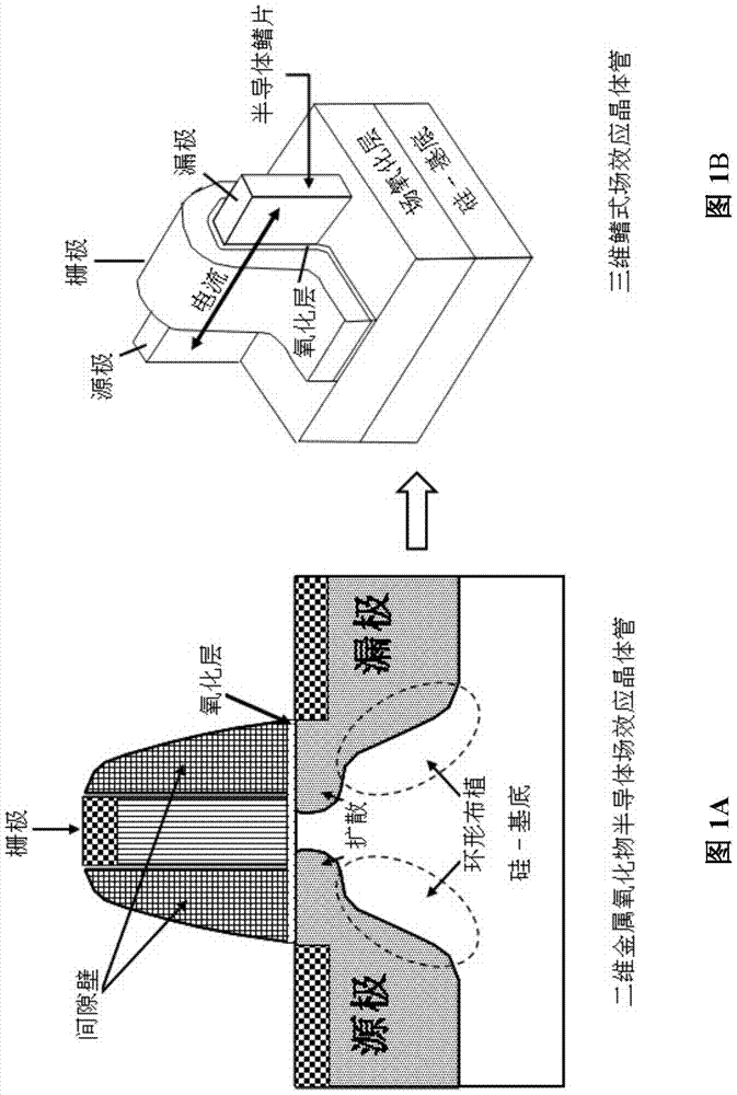
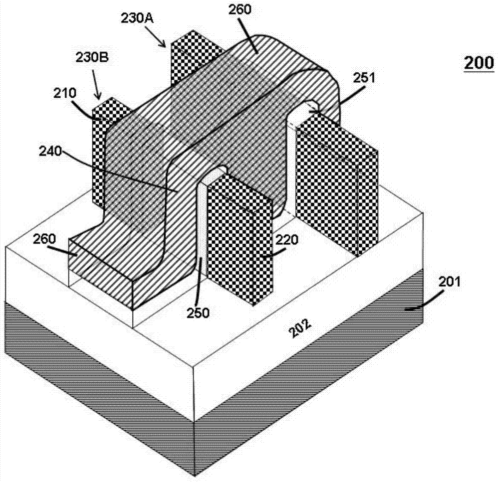
[0029] In order to meet the requirements of the embedded non-volatile memory storage in the CMOS process technology generation below 20 nanometers in the prior art, the present invention provides a semiconductor NVM device based on the three-dimensional fin field effect transistor process technology. The three-dimensional single floating gate non-volatile memory (SFGNVM) device of the present invention is a single-gate device and is fully compatible with the three-dimensional FinFET process. In the process technology of the present invention, no new process or non-traditional materials are introduced . At the same time, because the SFGNVM device...


PUM


Abstract

A 3-D Single Floating Gate Non-Volatile Memory (SFGNVM) device based on the 3-D fin Metal-Oxide-Semiconductor Field Effect Transistor (MOSFET) is disclosed. The disclosed Non-Volatile Memory (NVM) device consists of a pair of semiconductor fins and one floating metal gate. The floating metal gate for storing electrical charges to alter the threshold voltage of the fin MOSFET crosses over the pair of semiconductor fins on top of coupling and tunneling dielectrics above the surfaces of the two semiconductor fins. One semiconductor fin with the same type impurity forms the control gate of the non-volatile memory device. The other semiconductor fin is doped with opposite type of impurity in the channel regions under the metal floating gate and with the same type of impurity in the source and drain regions on the sides of the crossed metal floating gate.

Description

technical field [0001] The present invention relates to a three-dimensional (3-Dimension, 3-D) semiconductor non-volatile memory (non-volatile memory, NVM) unit device (cell device). The semiconductor non-volatile memory unit device of the present invention can be applied to the manufacture of standard complementary metal-oxide-semiconductor field effect transistors (complementary metal-oxide-semiconductor field effect transistors, CMOSFETs) of process technology generation (process technology node) below 20 nanometers The advanced fin field effect transistor (fin-shape field effect transistor, finFET) process technology is used for fabrication. In particular, the three-dimensional single floating gate non-volatile memory (single floating gate NVM, SFGNVM) device of the present invention is composed of a metal floating gate for storing charges (charge) and two MOSFET main body (body) and The control gate (control gate) is composed of semiconductor fins (fin). Background tec...

Claims


Application Information

Patent Timeline
Patent Type & Authority Applications(China)
IPC IPC(8): H01L27/115
CPCH01L29/7881H01L27/1156H01L29/42324H01L29/785H10B41/60H10B41/70
Inventor 王立中
Owner XINLIJIA INTEGRATED CIRCUIT (HANGZHOU) CO LTD
Why Eureka
Try Eureka