Electroluminescent Organic Transistor

An organic transistor and luminescence technology, applied in the direction of electric solid-state devices, circuits, electrical components, etc., can solve the problems of limiting the brightness and efficiency of devices, and achieve the effects of balancing differences, maximizing current density, and maximizing charge accumulation

Active Publication Date: 2016-04-06
FLEXTERRA INC
View PDF7 Cites 0 Cited by
  • Summary
  • Abstract
  • Description
  • Claims
  • Application Information

AI Technical Summary

Problems solved by technology

This inherent feature of the known device limits the thickness of the semiconductor layer in which the light is formed to a few molecular layers, thereby limiting the intensity of the light produced by the device
[0007] Furthermore, the intrinsic properties of this known device cause a significant quenching phenomenon of the excitons due to the interaction between said excitons and the free charges in the channel of the transistor, and thus limit the brightness and efficiency of the device

Method used


Image

  • Electroluminescent Organic Transistor

Examples


Embodiment Construction

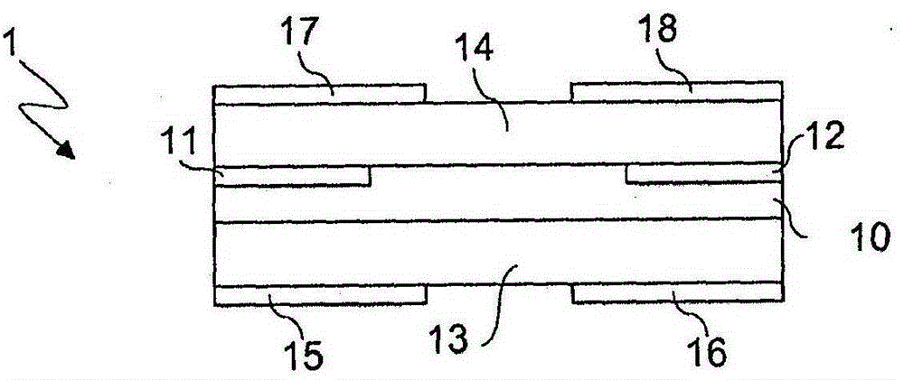
[0018] refer to figure 1 , showing that the electroluminescent organic transistor 1 according to the invention comprises at least one organic ambipolar semiconductor layer 10 suitable for a first type of charge (eg electrons) and a second type of charge (eg holes) transport and radiative recombination.

[0019] A source electrode 11 suitable for injection of the first type of charge (such as electrons) and a source electrode 11 suitable for the injection of the second type of charge (such as holes) are arranged in contact with the organic ambipolar semiconductor layer 10. injected into the drain electrode 12 .

[0020] The group formed by said organic ambipolar semiconductor layer 10 and said source electrode 11 and drain electrode 12 in contact with said layer 10 is arranged between two layers of dielectric material 13 and 14 .

[0021] The electroluminescence organic transistor 1 according to the present invention further comprises a first control electrode 15 and a second...


PUM


Abstract

The invention relates to a field-effect electroluminescent bipolar organic transistor (1) in which there are two pairs of control electrodes (15-18), a layer of bipolar electrodes in direct contact with the source (11) and drain (12) electrodes an organic semiconductor (10) and two separate dielectric layers (13, 14), and wherein each of said dielectric layers (13, 14) is arranged between a bipolar organic semiconductor layer (10) and a pair of control Between the electrodes (15-18).

Description

technical field [0001] The present invention relates to electroluminescent organic transistors. Background technique [0002] In the field of organic electronics, organic light-emitting diodes (OLEDs) have been extensively studied and many structural embodiments have been developed in order to obtain devices based on them. [0003] Application JP2003100457 discloses some semiconductor structures suitable for use as diodes, wherein additional control electrodes can be positioned vertically with respect to the substrate of the device (ie with respect to a multilayer semiconductor structure) in order to improve the injection and transport of charges. First, from a manufacturing point of view, it is clear that the multi-electrode structures of JP2003100457 are limited by their complexity. [0004] A scientific publication titled "Materials for high performance single layer OLED device" by Huang et al. in Significant Research Achievements of Academia Sinica Vol. 96 (2007) pp. 13...

Claims


Application Information

Patent Timeline
Patent Type & Authority Patents(China)
IPC IPC(8): H01L51/52
CPCH10K10/486H10K50/30H10K50/805
Inventor M·默西尼R·卡佩立S·托法尼
Owner FLEXTERRA INC
Why Eureka
Try Eureka