Touch liquid crystal display and array substrate thereof

A liquid crystal display and array substrate technology, which is applied in the field of touch liquid crystal display and touch liquid crystal display array substrate, can solve the problems of increasing the process difficulty of touch liquid crystal display, reducing the pixel aperture ratio, and increasing the defective process, so as to reduce the number of lines The effect of layout density, reducing the number of times the process is performed, and reducing the difficulty of the process

Inactive Publication Date: 2014-04-16
TCL CHINA STAR OPTOELECTRONICS TECH CO LTD
View PDF4 Cites 38 Cited by
  • Summary
  • Abstract
  • Description
  • Claims
  • Application Information

AI Technical Summary

Problems solved by technology

[0004] like figure 1 As shown, the prior art in-cell (In-Cell) voltage-sensing touch liquid crystal display adopts a set of independent scanning addressing circuits (including touch emission lines 41 and touch sensing lines 42 ) to realize the touch function. However, since the pixel structure of the liquid crystal display already has a set of scanning addressing lines for display functions (including horizontal gate lines 51 and vertical data lines 52), when used as a display When the functional gate lines 51 and data lines 52 are interlaced with the touch emission lines 41 and touch sensing lines 42 used as touch functions, not only the aperture ratio of the pixels is reduced, but also the cost of preparing the touch liquid crystal display is increased. The process is difficult, and the corresponding process defects will also increase; in addition, since the touch sensing line 42 is adjacent to the data line 52 and the distance is very close, the interference between signals will be further increased

Method used


Image

  • Touch liquid crystal display and array substrate thereof
  • Touch liquid crystal display and array substrate thereof
  • Touch liquid crystal display and array substrate thereof

Examples


Embodiment Construction

[0033] The following descriptions of the various embodiments refer to the accompanying drawings to illustrate specific embodiments in which the present invention can be implemented. The directional terms mentioned in the present invention, such as "up", "down", "front", "back", "left", "right", "inside", "outside", "side", etc., are for reference only The orientation of the attached schema. Therefore, the directional terms used are used to illustrate and understand the present invention, but not to limit the present invention.

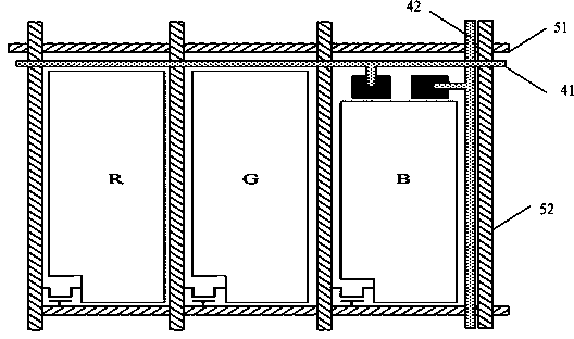
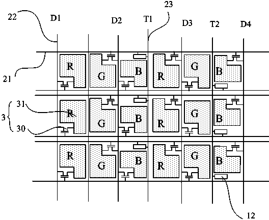
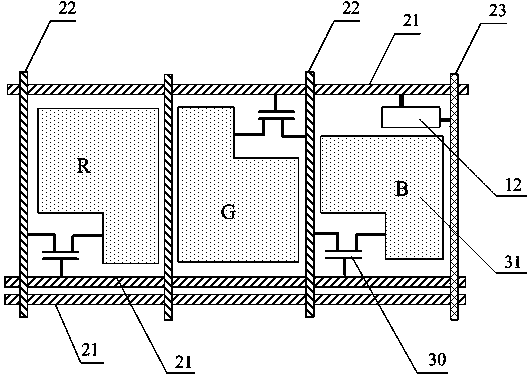
[0034] Such as figure 2 as well as image 3 As shown, an embodiment of the touch liquid crystal display array substrate of the present invention is shown, in this embodiment, the touch liquid crystal display array substrate includes a plurality of pixels defined by a plurality of gate lines 21 and a plurality of data lines 22 Unit 3, a thin film transistor 30 and a pixel electrode 31 are formed in each pixel unit 3 (see D1 to D4 in the figure); whe...


PUM


Abstract

Embodiments of the invention disclose a touch liquid crystal display array substrate comprising a plurality of pixel units defined by gate lines and data lines. A thin-film transistor and a pixel electrode are formed in each pixel unit. The array substrate further comprises touch circuit units used for touch positioning. Each touch circuit unit comprises a touch emitting line, a touch sensing line, and a photosensitive unit; the touch emitting line and the touch sensing line interest with each other; the photosensitive unit disposed at an intersection is connected with both the touch emitting line and the touch sensing line; the touch emitting line is one gate line; the touch sensing line is one dummy data line arranged on the array substrate; the dummy data line and one adjacent data line are spaced by at least one pixel electrode. The embodiments correspondingly disclose a touch liquid crystal display. Through the application of the embodiments, pixel aperture ratio can be increased, touch positioning sensitivity is improved, and product yield is increased.

Description

technical field [0001] The present invention relates to the field of thin film transistor liquid crystal display (Thin Film Transistor liquid crystal display, TFT-LCD), in particular to a touch liquid crystal display array substrate and a corresponding touch liquid crystal display. Background technique [0002] Liquid crystal display (liquid crystal display, LCD) technology has developed rapidly, and great progress has been made from the size of the screen to the quality of the display. LCD has the characteristics of small size, low power consumption, and no radiation. Dominance in the field of flat panel displays. [0003] The touch LCD screen is one of the important carriers that integrate the input and output terminals. In recent years, demand for touch-screen LCDs has surged with the advent of a range of products, including small, lightweight handheld devices. [0004] Such as figure 1 As shown, the prior art in-cell (In-Cell) voltage-sensing touch liquid crystal disp...

Claims


Application Information

Patent Timeline
Patent Type & Authority Applications(China)
IPC IPC(8): G02F1/1333
CPCG02F1/13338G06F3/042G06F3/0412G02F1/13318G02F1/133514G02F1/134309G02F1/136286G02F1/1368G06F3/0421G06F3/047
Inventor 徐向阳
Owner TCL CHINA STAR OPTOELECTRONICS TECH CO LTD
Why Eureka
Try Eureka