Drilling method of circuit board

A drilling method and circuit board technology, which is applied to printed circuits, printed circuit manufacturing, electrical components, etc., can solve the problems of low hole position accuracy, inability to drill through PCB boards at one time, and PCB board scrapping, so as to avoid hole position Errors, avoid weakening of resistance to deformation, and ensure high-precision effects

Active Publication Date: 2016-09-21
GUANGZHOU FASTPRINT CIRCUIT TECH +2
View PDF5 Cites 0 Cited by
  • Summary
  • Abstract
  • Description
  • Claims
  • Application Information

AI Technical Summary

Problems solved by technology

At present, the drilling process of PCB boards is to use a drill to completely drill through from one side of the PCB to the other. For PCB boards with a high thickness-to-diameter ratio, when using ordinary drills to drill holes, it is limited by the length of the blade and cannot be drilled at one time. When using a drill with a longer edge length, it is easy to break because the strength of the drill is reduced. Once the drill is broken, it is difficult to take it out from the PCB, and the PCB will inevitably be scrapped.
Moreover, board thickness is a very critical factor affecting the accuracy of the hole position. The thicker the PCB board, the lower the accuracy of the drilled hole position, especially the reverse side. As the thickness of the uncut material becomes thinner, it resists deformation. The ability to gradually weaken, resulting in the accuracy of the opposite face will become very poor
Therefore, it is difficult to achieve the problem of obtaining high-precision hole positions for such high-thickness-diameter-ratio PCB boards with general drilling methods.

Method used


Image

  • Drilling method of circuit board

Examples


Embodiment Construction

[0023] The present invention will be described in detail below with reference to the accompanying drawings and specific embodiments.

[0024] A drilling method for a circuit board, comprising the following steps:

[0025] 1. Setting of positioning target and direction target.

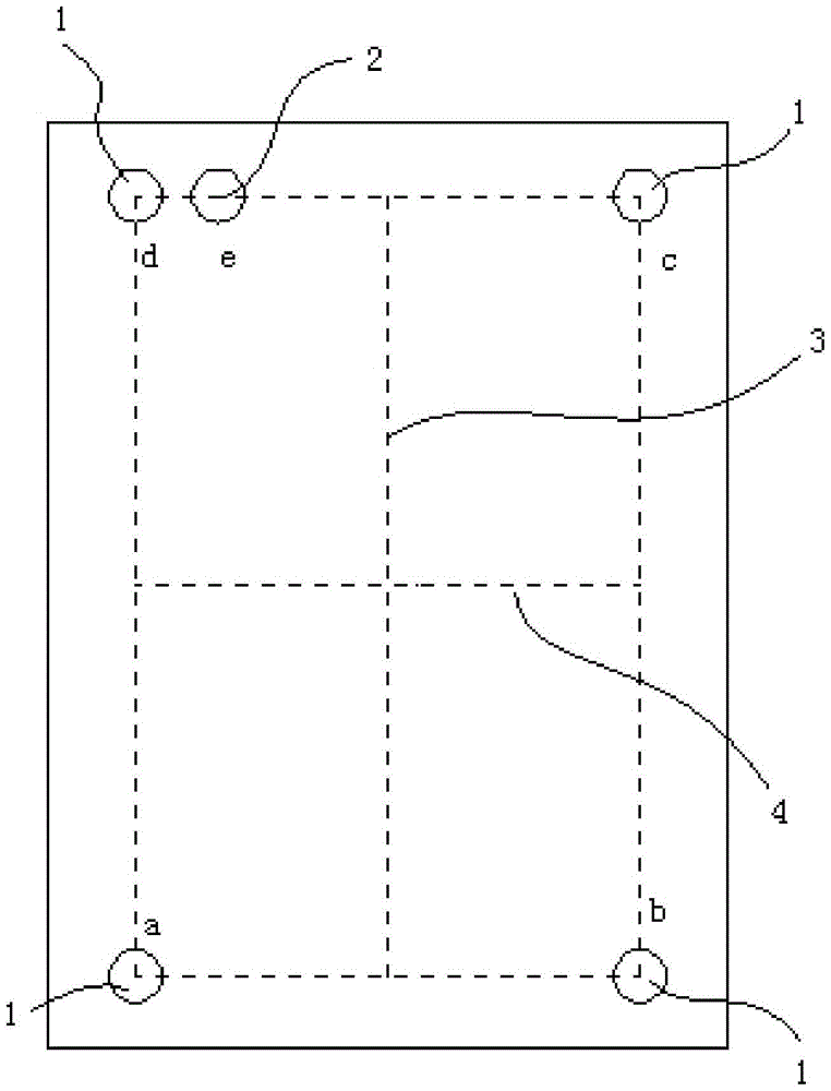
[0026] like figure 1 As shown, a positioning target 1 and a direction target 2 are set on the circuit board, and the positioning targets 1 are four, which are respectively set in the four corner directions of the circuit board, and the four positioning targets 1 are the endpoints. Positioning graphics that make up a rectangle. The direction target 2 is one, which is located on one side of the rectangular positioning figure, and is a positioning target close to the end point of the side, with a distance of 5-6 mm from the positioning target.

[0027] According to the above design, when the inner layer pattern is produced, the patterns of the positioning target and the direction target are produced on ...


PUM

PropertyMeasurementUnit
lengthaaaaaaaaaa
thicknessaaaaaaaaaa

Abstract

A drilling method for a circuit board, comprising the following steps: arranging positioning targets (1) and a direction target (2) on a circuit board, and drilling positioning holes at the positioning targets (1) and a direction hole at the direction target (2), using the direction hole to identify the direction of the circuit board; drilling respectively from the front side and the rear side of the circuit board, so that the drill holes of the front side and the rear side form through holes. The present drilling method can achieve drilling of a circuit board with a high thickness to diameter ratio, and can obtain high accuracy hole positions.

Description

technical field [0001] The invention relates to a method for preparing a circuit board, in particular to a method for drilling a circuit board. Background technique [0002] Drilling is a very important process in the PCB manufacturing process. Drilling on the circuit board is mainly used for the welding of circuit board components and the conduction between layers. At present, the drilling process of PCB board is to use a drill to completely drill through from one side of the PCB to the other side. For PCB boards with high aspect ratio, when drilling with ordinary drills, it is limited by the length of the blade and cannot be drilled once. When using a drill with a longer blade length, it is easy to break because the strength of the drill is reduced. Once the drill is broken, it is difficult to remove it from the PCB board, which will inevitably make the PCB board scrapped. In addition, the thickness of the board is a very critical factor affecting the hole position accura...

Claims


Application Information

Patent Timeline
Patent Type & Authority Patents(China)
IPC IPC(8): B23B35/00
CPCH05K3/0047H05K2203/1476H05K2203/167
Inventor 任小浪陈蓓樊光辉
Owner GUANGZHOU FASTPRINT CIRCUIT TECH
Why Eureka
Try Eureka