Array substrate, liquid crystal display panel and display device

A technology of an array substrate and a substrate substrate, applied in the field of display devices, can solve the problems of waste, low utilization rate of light energy of a display panel, etc., and achieve the effect of improving utilization rate

Inactive Publication Date: 2014-04-30
BEIJING BOE OPTOELECTRONCIS TECH CO LTD +1
View PDF8 Cites 17 Cited by
  • Summary
  • Abstract
  • Description
  • Claims
  • Application Information

AI Technical Summary

Problems solved by technology

[0003] At present, the existing liquid crystal display panel only utilizes the light energy passing through the light-transmitting area, and the light energy blocked by the light-shielding area is in a waste state, so the light energy utilization rate of the existing liquid crystal display panel is low

Method used


Image

  • Array substrate, liquid crystal display panel and display device
  • Array substrate, liquid crystal display panel and display device
  • Array substrate, liquid crystal display panel and display device

Examples


Embodiment Construction

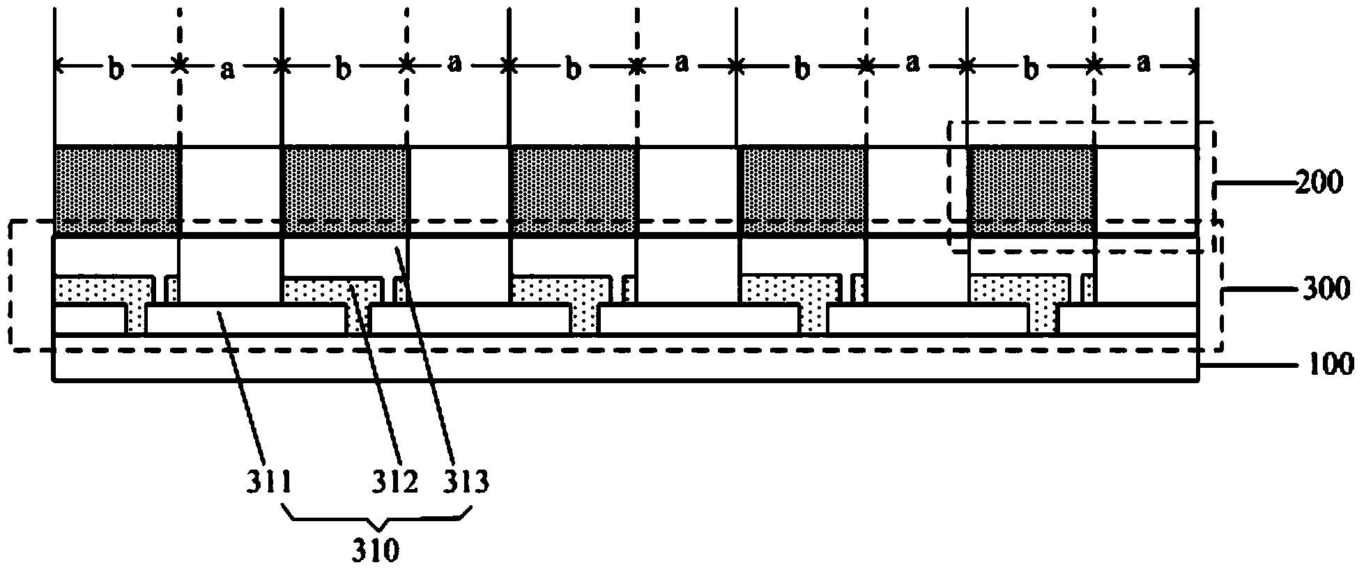
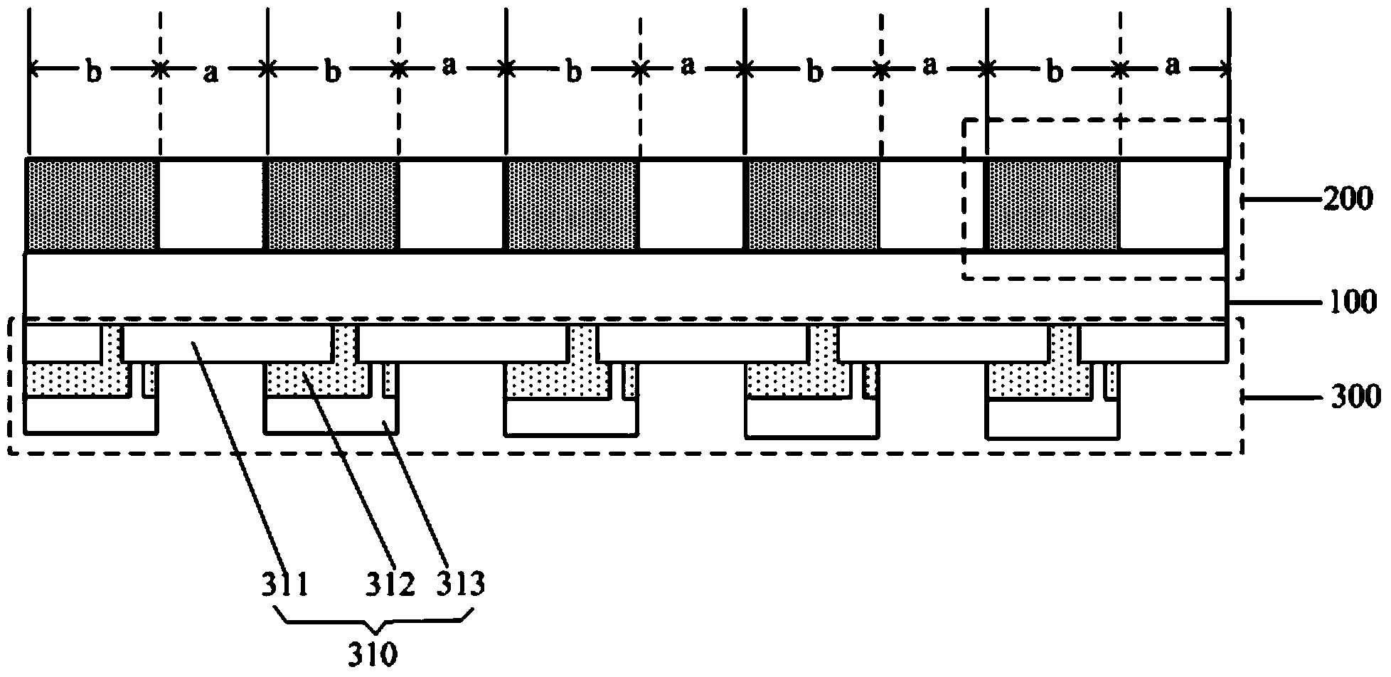
[0028] The specific implementation manners of the array substrate, the liquid crystal display panel and the display device provided by the embodiments of the present invention will be described in detail below with reference to the accompanying drawings.

[0029] The size and shape of each component in the drawings do not reflect the real scale of the array substrate, but are only intended to schematically illustrate the content of the present invention.

[0030] An array substrate provided by an embodiment of the present invention, such as Figure 1a with Figure 1b As shown, it includes a base substrate 100, a plurality of pixel units 200 disposed on the base substrate 100 and arranged in a matrix, and a driving module ( Figure 1a with Figure 1b The structure of the driving module is not shown in ,); each pixel unit 200 is divided into a light-transmitting area a and a light-shielding area b, and also includes:

[0031] A photovoltaic cell assembly 300 electrically connec...


PUM


Abstract

The invention discloses an array substrate, a liquid crystal display panel and a display device. The array substrate comprises a substrate, a plurality of pixel units arranged on the substrate, a driving module for providing displaying signals to each pixel unit and a photovoltaic cell pack electrically connected with the driving module, the photovoltaic cell pack comprises a plurality of photovoltaic cells, each of the photovoltaic cells comprises a first transparent electrode, a photovoltaic thin film and a second transparent electrode, and the orthographic projection of the photovoltaic thin film on the substrate is inside a shading area. Since the photovoltaic cell pack electrically connected with the driving module is arranged in the array substrate, the photovoltaic cell pack can be utilized to convert luminous energy in the shading area into electric energy, and outputs the electric energy to the driving module for use, the luminous energy in the shading area can be effectively utilized to increase using rate of luminous energy by the array substrate. Since the orthographic projection of the photovoltaic thin film on the substrate is inside the shading area, aperture opening rate of each pixel unit in the array substrate is not affected.

Description

technical field [0001] The invention relates to the field of display technology, in particular to an array substrate, a liquid crystal display panel and a display device. Background technique [0002] Thin Film Transistor-Liquid Crystal Display (TFT-LCD) occupies a dominant position in the current display panel market due to its small size, low power consumption, and no radiation. A thin film transistor liquid crystal display panel is mainly composed of an array substrate, an opposite substrate, liquid crystal molecules located between the two substrates, and a backlight source. Wherein, a plurality of pixel units arranged in a matrix are arranged on the array substrate, and thin film transistors, metal signal lines, and pixel electrodes are arranged in each image unit. In each pixel unit, the area through which light in the backlight can pass is generally called a light-transmitting area, and the area where light in the backlight cannot pass through is called a light-shiel...

Claims


Application Information

Patent Timeline
Patent Type & Authority Applications(China)
IPC IPC(8): G02F1/1333G02F1/13H01L27/12
CPCH01L27/12G02F1/1313H01L2924/0002G02F1/13324H01L2924/00G02F1/133357G02F1/134345G02F1/13318G02F1/133555G02F1/134309G02F1/13439G02F1/1368H01L25/167
Inventor 沈奇雨陈旭郭建
Owner BEIJING BOE OPTOELECTRONCIS TECH CO LTD
Why Eureka
Try Eureka