Array substrate, capacitive touch screen and touch display device

An array substrate and substrate technology, which is applied to static indicators, electrical digital data processing, optics, etc., can solve the problems of increasing the manufacturing cost and manufacturing difficulty, high manufacturing cost and low production efficiency of capacitive in-line touch screens, and achieves a high level of production efficiency. The effect of helping electric field projection, simple preparation process and improving production efficiency

CN103760708AActive Publication Date: 2014-04-30BEIJING BOE OPTOELECTRONCIS TECH CO LTD +1
5 Cites 39 Cited by

Patent Information

Authority / Receiving Office
CN · China
Patent Type
Applications(China)
Current Assignee / Owner
Publication Date
2014-04-30

Smart Images

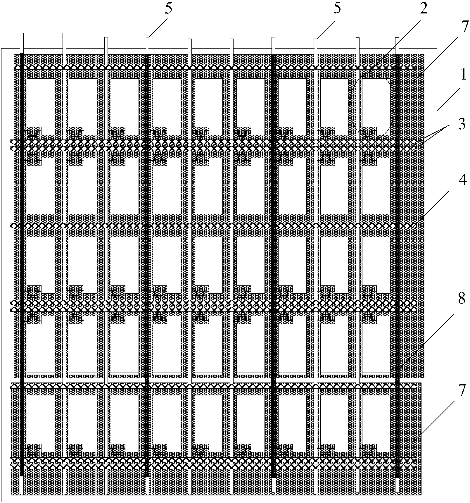
  • Figure 1
    Figure 1
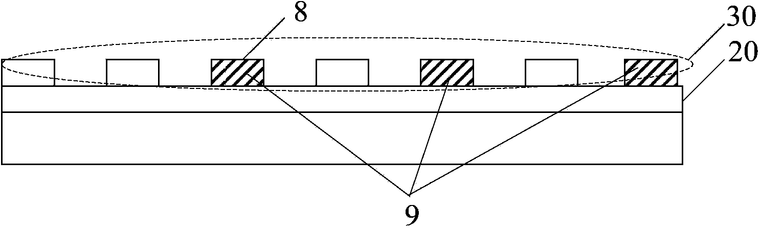
  • Figure 2
    Figure 2
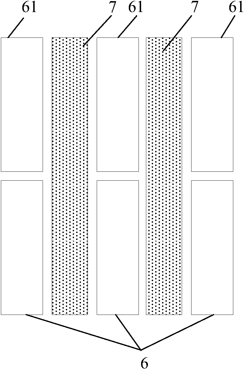
  • Figure 3
    Figure 3
Patent Text Reader

Abstract

The invention discloses an array substrate, a capacitive touch screen and a touch display device. A common electrode layer of the array substrate comprises a plurality of touch drive electrodes and a plurality of common electrodes; the touch drive electrodes and the common electrodes are intersected; the touch drive electrodes extend in a column direction; the common electrodes extend in a row direction. A pixel electrode layer of the array substrate comprises a plurality of first leads; projections of the first leads on the array substrate locate in an area of the common electrodes and right face data line positions in the area of the common electrodes; the first leads having the projections locating in the area of the same common electrode form one touch drive electrode. The touch drive electrodes and touch sensing electrodes are arranged on the common electrode layer and the pixel electrode layer respectively, the array substrate with the touch function can be manufactured without adding manufacturing processes during manufacturing, the manufacturing process is simple, production cost is reduced, and production efficiency is improved.
Need to check novelty before this filing date? Find Prior Art

Description

technical field

[0001] The present invention relates to the field of display technology, in particular to an array substrate, a capacitive embedded touch screen and a touch display device. Background technique

[0002] According to the composition and structure, the touch screen can be divided into: Add on Mode Touch Panel, On Cell Touch Panel, and In Cell Touch Panel. Among them, the plug-in touch screen is produced separately from the touch screen and Liquid Crystal Display (LCD), and then bonded together to form an LCD screen with touch function. The production cost of the plug-in touch screen is relatively high, and the light transmittance is low. 1. The module is thicker; the surface-covering touch screen also has the problem of thicker modules. The capacitive in-cell touch screen embeds the touch drive electrodes of the touch screen inside the liquid crystal display. Because it implements the touch sensing circuit in the box, the module can be made thinner and lighter...

Examples

Embodiment Construction

[0028] The implementation process of the embodiment of the present invention will be described in detail below in conjunction with the accompanying drawings. It should be noted that the same or similar reference numerals represent the same or similar elements or elements having the same or similar functions throughout. The embodiments described below by referring to the figures are exemplary only for explaining the present invention and should not be construed as limiting the present invention.

[0029] see figure 1 , the embodiment of the present invention provides an array substrate, including a substrate 1, on which a plurality of pixel units 2 arranged in a matrix are formed, and gate signal lines 3 and common electrode signal lines 4 are arranged in the row direction. A data line 5 is arranged between the column pixel units 2 .

[0030] see figure 2 As shown, a common electrode layer 20 and a pixel electrode layer 30 are also included.

[0031] combine figure 1 and ...