Silicon wafer cleaning process

A silicon wafer cleaning and process technology, applied in cleaning methods and utensils, cleaning methods using liquids, chemical instruments and methods, etc., can solve the problems of ineffective removal of metals, weak reaction ability, easy adsorption of particle impurities, etc.

Inactive Publication Date: 2014-04-30
SHANGHAI SHENHE THERMO MAGNETICS ELECTRONICS CO LTD
View PDF3 Cites 15 Cited by
  • Summary
  • Abstract
  • Description
  • Claims
  • Application Information

AI Technical Summary

Problems solved by technology

[0002] In the field of silicon wafer cleaning, DHF (HF+H 2 O) As one of the standard processes, it has been used for a long time. Its function of removing surface metal is mainly in the HF tank. Since HF is a weak acid, and because it can react with the surface's own oxide film, the surface of the silicon wafer is hydrophobic. In summary, there are the following disadvantages: 1. Weak acid HF cannot effectively remove more active metals such as Na, K, Ca, Mg, Zn, Al; 2. The surface of silicon

Method used


Image

  • Silicon wafer cleaning process
  • Silicon wafer cleaning process

Examples


Embodiment Construction

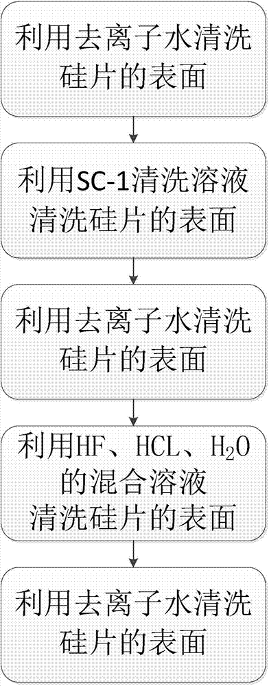
[0012] The silicon wafer cleaning process of the present invention will be described in further detail below in conjunction with the accompanying drawings.

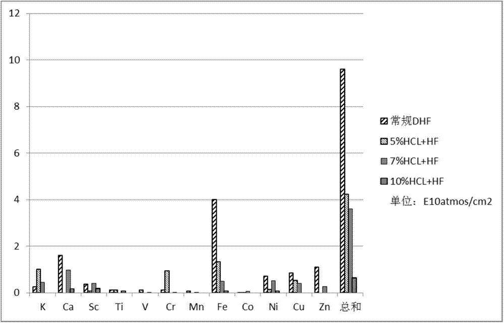
[0013] Such as figure 1 As shown, in the silicon wafer cleaning process of the present invention, the first step is to clean the surface of the silicon wafer with deionized water. The second step is to use SC-1 cleaning solution to clean the surface of the silicon wafer to remove particulate organic matter, etc. In order to improve the cleaning effect and enhance the removal ability, a multi-tank cleaning method is adopted. The third step is to use deionized water to clean the surface of the silicon wafer to remove the liquid medicine in the previous tank. In order to improve the cleaning effect and enhance the removal ability, a multi-tank cleaning method is adopted. The fourth step, using HF, HCL, H 2 The mixed solution of O cleans the surface of the silicon wafer, in which HF, HCL, H 2 The ratio of O mixed solution ...


PUM


Abstract

The invention discloses a silicon wafer cleaning process. The silicon wafer cleaning process comprises the following steps of (1) using deionized water to clean the surface of a silicon wafer, (2) using an SC-1 cleaning solution to clean the surface of the silicon wafer, (3) using deionized water to clean the surface of the silicon wafer, (4) using a mixed solution containing HF, HCL and H2O to clean the surface of the silicon wafer, and (5) using deionized water to clean the surface of the silicon wafer. According to the silicon wafer cleaning process, due to the fact that the HCL is added to DHF, acidity of the DHF is improved, the metal attachment phenomenon in cleaning fluid cannot easily happen in the high-acidity solution, and the high capacity of removing metal on the surface of the silicon wafer is achieved; compared with a DHF process, the silicon wafer cleaning process has the three advantages that Na, K, Ca, Mg and Al can be further and effectively removed through the HCL; the PH value of the solution of the HCL is lowered, the state of metal complexing ions in the cleaning fluid is controlled, and reattachment of metal is inhibited; the content of Cu2O and the content of CuO on the surface of the silicon wafer can be reduced, and thus the content of Cu on the whole surface of the silicon wafer is controlled.

Description

technical field [0001] The invention belongs to the field of semiconductor manufacturing, and relates to a novel polishing wafer surface metal control technology, in particular to a silicon wafer cleaning process. Background technique [0002] In the field of silicon wafer cleaning, DHF (HF+H 2 O) As one of the standard processes, it has been used for a long time. Its function of removing surface metal is mainly in the HF tank. Since HF is a weak acid, and because it can react with the surface's own oxide film, the surface of the silicon wafer is hydrophobic. In summary, there are the following disadvantages: 1. Weak acid HF cannot effectively remove more active metals such as Na, K, Ca, Mg, Zn, Al; 2. The surface of silicon wafers after HF cleaning is hydrophobic and cannot be ideal. The surface is relatively active and easy to absorb particles and impurities. [0003] Since FTS currently uses DHF (mainly HF) to remove silicon wafer metal, the principle is: use HF to clea...

Claims


Application Information

Patent Timeline
IPC IPC(8): H01L21/02B08B3/08
CPCH01L21/02068B08B3/08
Inventor 金文明贺贤汉张恩泽吴佳明
Owner SHANGHAI SHENHE THERMO MAGNETICS ELECTRONICS CO LTD
Why Eureka
Try Eureka