BGA (ball grid array) ball-mounting method
A technology of planting balls and solder balls, applied in the direction of tin feeding devices, electrical components, circuits, etc., can solve the problems of inappropriate low-cost production, complicated adjustment of production process parameters, and high cost of packaging chip sample development
- Summary
- Abstract
- Description
- Claims
- Application Information
AI Technical Summary
Problems solved by technology
Method used
Image
Examples
Embodiment Construction
[0027] In order to make the content of the present invention clearer and easier to understand, the content of the present invention will be described in detail below in conjunction with specific embodiments and accompanying drawings.
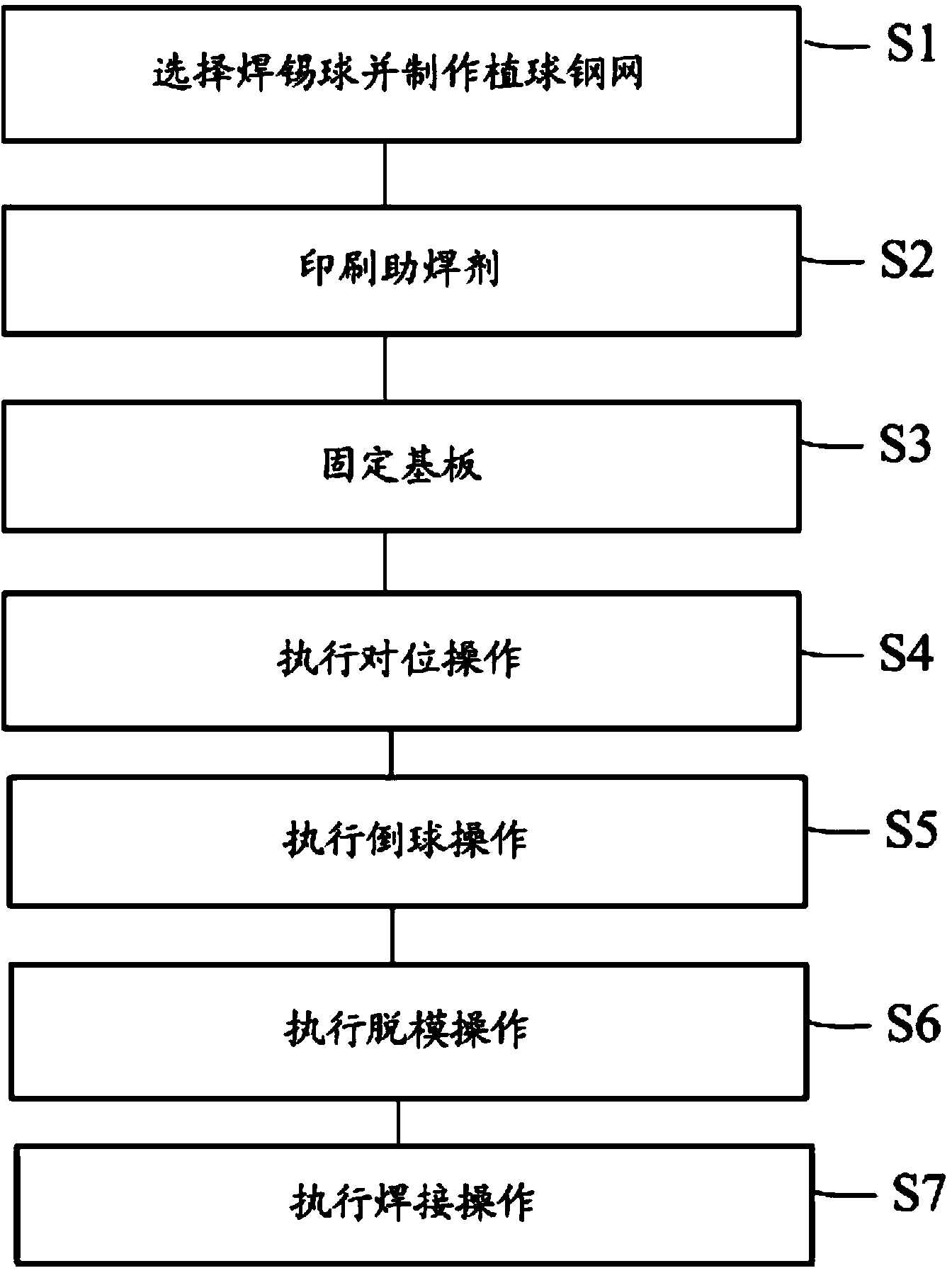
[0028] image 3 A flow chart of a BGA ball planting method according to a preferred embodiment of the present invention is schematically shown.
[0029] Specifically, as image 3 As shown, the BGA ball planting method according to a preferred embodiment of the present invention includes:
[0030] The first step S1 is to select solder balls and make a ball planting stencil, wherein according to the size and spacing of the pads on the BGA substrate, select the corresponding solder balls and make the ball planting stencil; specifically, for example, according to The spacing, array and diameter of the solder balls of the BGA package substrate pads, and design and manufacture a special ball-planting stencil, so that the spacing and array of the ste...
PUM
 Abstract
Description
Claims
Application Information


