Optical proximity correction method for contact hole graphic design

A technology of optical proximity correction and graphic design, which is applied in the direction of photo-plate making process of originals for photomechanical processing, optics, pattern surface, etc., and can solve problems such as not reaching the size and affecting the performance of the circuit

Active Publication Date: 2014-05-07
SEMICON MFG INT (SHANGHAI) CORP
View PDF7 Cites 11 Cited by
  • Summary
  • Abstract
  • Description
  • Claims
  • Application Information

AI Technical Summary

Problems solved by technology

However, due to the limitations of the mask rule inspection, the above-mentioned optical proximity correction of the contact hole pattern has an impact, resulting in that the corrected contact hole pattern cannot reach the designed target when it is realized on the mask plate and then transferred to the test silicon wafer. size, which ultimately affects the performance of the overall circuit

Method used


Image

  • Optical proximity correction method for contact hole graphic design
  • Optical proximity correction method for contact hole graphic design
  • Optical proximity correction method for contact hole graphic design

Examples


Embodiment Construction

[0018] In the following description, numerous specific details are given in order to provide a more thorough understanding of the present invention. It will be apparent, however, to one skilled in the art that the present invention may be practiced without one or more of these details. In other examples, some technical features known in the art are not described in order to avoid confusion with the present invention.

[0019] In order to thoroughly understand the present invention, detailed steps will be presented in the following description to illustrate the optical proximity correction method for contact hole pattern design proposed by the present invention. Obviously, the practice of the invention is not limited to specific details familiar to those skilled in the semiconductor arts. Preferred embodiments of the present invention are described in detail below, however, the present invention may have other embodiments besides these detailed descriptions.

[0020] It shoul...


PUM


Abstract

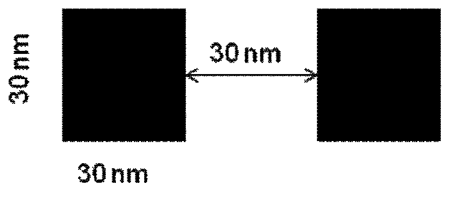
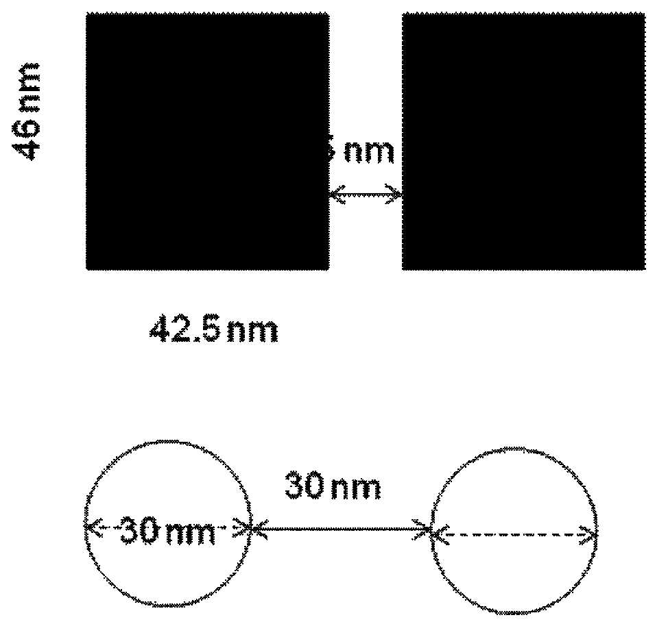
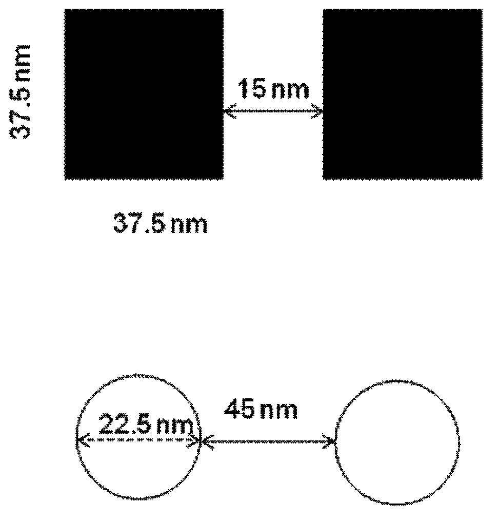
The invention provides an optical proximity correction method for contact hole graphic design, and the method comprises the following steps: providing a design layout with contact hole graph; implementing a first optical proximity correction for the contact hole figure in the design layout; determining whether the contact hole figure after the first optical proximity correction satisfies the requirement of mask layer rule examination, if the contact hole figure does not satisfy the requirement of mask layer rule examination, implementing a second optical proximity correction for the contact hole figure which is processed by the first optical proximity correction, and simultaneously adding another figure between the contact hole figures which are processed by the first optical proximity correction, and thereby connecting the two adjacent contact hole figures for forming a figure unit; carrying out a photoetching projection simulation for the figure unit. According to the invention, the optical proximity correction for the contact hole figure is not limited by the mask layer rule examination, and thereby the corrected contact hole figure can completely compensate the deformation of the contact hole figure caused by interference and diffraction of light during photoetching simulation.

Description

technical field [0001] The invention relates to a semiconductor manufacturing process, in particular to a method for optical proximity correction (OPC) for contact hole pattern design. Background technique [0002] Integrated circuits have developed from large-scale, ultra-large-scale to very large-scale. Correspondingly, the semiconductor manufacturing process has made great progress, and the feature size of the circuit is getting smaller and smaller, which is close to or smaller than the wavelength of light in the photolithography process. According to the principle of light interference and diffraction, when the light irradiates the mask pattern on the silicon wafer, the pattern will be deformed due to the mutual optical proximity effect (Optical Proximity Effects, OPE), which will lead to the reduction of circuit performance and even logic. mistake. Therefore, some correction methods must be used to compensate for the graphic deformation caused by the optical proximity...

Claims


Application Information

Patent Timeline
Patent Type & Authority Applications(China)
IPC IPC(8): G03F1/36
Inventor 王辉王伟斌
Owner SEMICON MFG INT (SHANGHAI) CORP
Why Eureka
Try Eureka