Optical module and detection circuit thereof

A detection circuit and optical module technology, applied in the field of optical communication, can solve the problems of unfavorable instrument miniaturization, wrong locking point, slow modulator locking speed, etc.

Active Publication Date: 2014-05-07
HUAWEI TECH CO LTD
View PDF4 Cites 4 Cited by
  • Summary
  • Abstract
  • Description
  • Claims
  • Application Information

AI Technical Summary

Problems solved by technology

However, the responsivity of different modulators varies greatly, resulting in slow locking speed of the modulator, jumping around the locking point, wrong locking point, etc.
[0004] The prior art also provides another detection circuit, which sets multiple sampling resistors and selects the sampling resistors through switches. In this case, although the adaptability to the responsiveness of the modulator can be improved, this In this case, the detection circuit is very complicated and takes up a lot of PCB area, which is not conducive to the miniaturization of the instrument.

Method used


Image

  • Optical module and detection circuit thereof
  • Optical module and detection circuit thereof
  • Optical module and detection circuit thereof

Examples


Embodiment Construction

[0021] In the following description, for purposes of illustration rather than limitation, specific details such as specific system architectures, interfaces, and techniques are set forth in order to provide a thorough understanding of the present application. It will be apparent, however, to one skilled in the art that the present application may be practiced in other embodiments without these specific details. In other instances, detailed descriptions of well-known devices, circuits, and methods are omitted so as not to obscure the description of the present application with unnecessary detail.

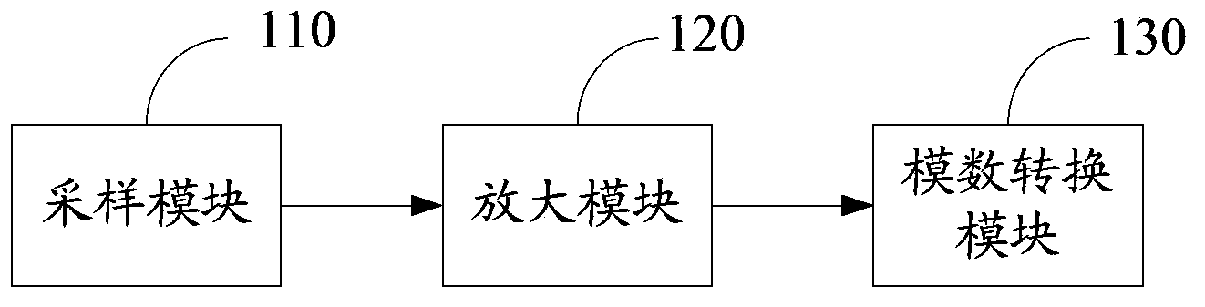
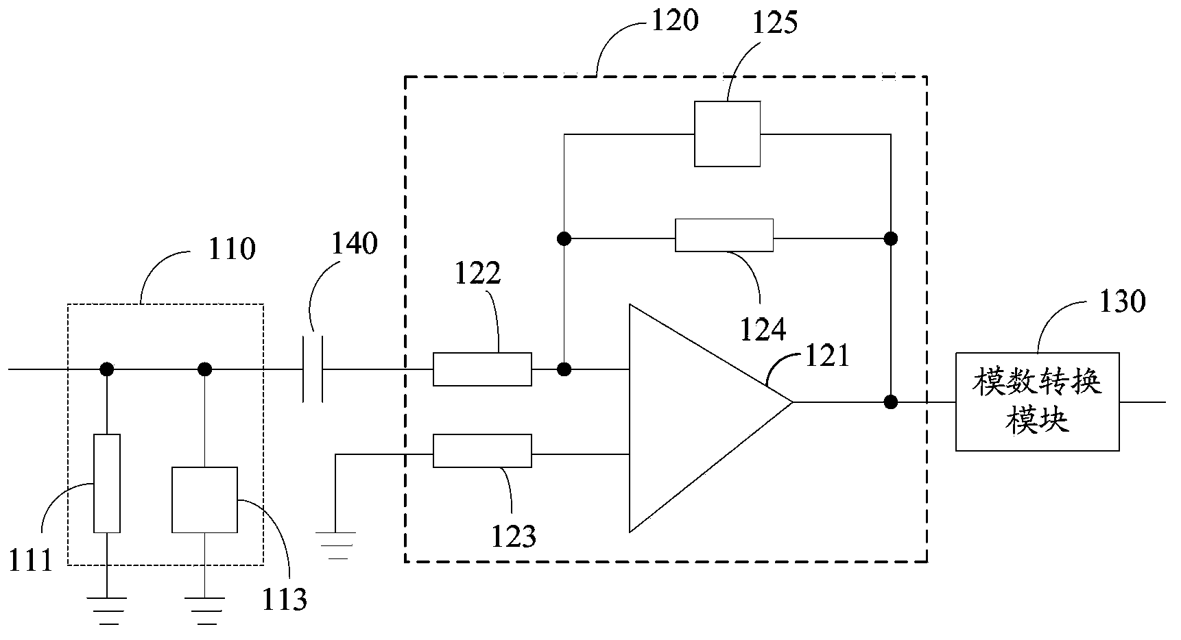
[0022] refer to figure 1 , figure 1 It is a structural schematic diagram of an embodiment of the detection circuit of the present application. The detection circuit in this embodiment includes: a sampling module 110 , an amplification module 120 and an analog-to-digital conversion module 130 . Wherein, the output end of the sampling module 110 is coupled to the input end of the am...


PUM


Abstract

The application discloses an optical module and a detection circuit thereof. The detection circuit comprises a sampling module which comprises a first potentiometer used for converting sampling current into sampling voltage; an amplification module which is coupled with the output end of the sampling module and used for amplifying the sampling voltage; and an analog-to-digital conversion module which is coupled with the output end of the amplification module and used for converting the amplified sampling voltage into a data signal to detect. The sampling module of the detection circuit is provided with the potentiometer which can adjust resistance of the sampling module so that responsibility of different modulators can be adapted, locking speed of the modulators can be enhanced, left and right jump of locking points and errors of the locking points can be prevented, and area occupied by a PCB can be reduced.

Description

technical field [0001] The present application relates to the field of optical communication, in particular to an optical module and a detection circuit thereof. Background technique [0002] When performing optical communication, the optical carrier must be sent to the modulator at the sending end for modulation to load data information on the optical carrier for transmission. However, modulators are usually mainly composed of simple optical elements, which are easily affected by changes in the external environment, thus affecting the output modulated signal. In order to reduce the influence of the outside world on the modulator, the DC bias point of the modulator must be changed as the outside world changes. Therefore, the signal at the output of the modulator must be detected. [0003] The prior art proposes a detection circuit, which converts the sampling current into a sampling voltage through a sampling resistor, and then feeds it back to the modulator. When the out...

Claims


Application Information

Patent Timeline
Patent Type & Authority Applications(China)
IPC IPC(8): H04B10/07
CPCH04B10/50575G01R19/00H04B10/588
Inventor 陈慰健汪永忠
Owner HUAWEI TECH CO LTD
Why Eureka
Try Eureka