Image sensor for pixel splitting and merging and signal transmission method of image sensor

An image sensor and signal technology, applied in the field of image sensors, can solve the problems of inappropriate ADC module system architecture, and achieve the effect of saving layout area, optimizing image quality, and reducing sampling frequency.

Active Publication Date: 2014-05-07
SHANGHAI INTEGRATED CIRCUIT RES & DEV CENT
View PDF8 Cites 25 Cited by
  • Summary
  • Abstract
  • Description
  • Claims
  • Application Information

AI Technical Summary

Problems solved by technology

However, due to the large layout area of ​​multiple ADC modules, this kind of pixel splitting and merging image sensor is suitable for sensors with larger pixels, and for image sensors with small pixels (such as pixel size below 2.5um), due to the The height of the ADC layout is only 2.5um or 5um, the system architecture of the above-mentioned multiple ADC modules is not suitable

Method used


Image

  • Image sensor for pixel splitting and merging and signal transmission method of image sensor
  • Image sensor for pixel splitting and merging and signal transmission method of image sensor
  • Image sensor for pixel splitting and merging and signal transmission method of image sensor

Examples


Embodiment Construction

[0042] In order to make the content of the present invention clearer and easier to understand, the content of the present invention will be further described below in conjunction with the accompanying drawings. Of course, the present invention is not limited to this specific embodiment, and general replacements known to those skilled in the art are also covered within the protection scope of the present invention.

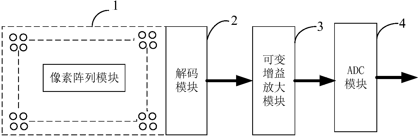
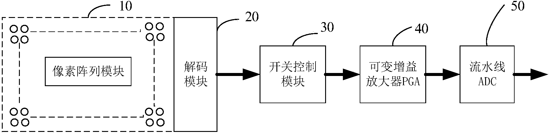
[0043] figure 2 is a block diagram of the image sensor of the present invention. Such as figure 2 As shown, the image sensor includes a pixel array module 10 , a decoding module 20 , a switch control module 30 , a variable gain amplifier PGA40 and a pipeline ADC50 . The pixel array module 10 may be a pixel array composed of a plurality of pixel groups, each pixel group includes a plurality of pixels, and the plurality of pixels constitute at least one unit pixel. A plurality of switch control modules 30 are arranged corresponding to each row of the pixel array...


PUM


Abstract

The invention discloses an image sensor which comprises a pixel array module formed by multiple pixel groups, multiple switch control modules, a variable gain amplifier, an assembly line ADC and a decoding module, wherein each pixel group comprises multiple pixels which constitute at least one unit pixel, each switch control module corresponds to one line of the pixel array module in configuration and comprises a first gating circuit and a second gating circuit, the variable gain amplifier processes output signals of the first gating circuits and output signals of the second gating circuits, the assembly line ADC carries out analog-to-digital conversion on the signals output by the variable gain amplifier, and the decoding module controls the first gating circuit and the second gating circuit of each line to be alternately read, outputs signals of various unit pixels of each line and controls the first gating circuits and the second gating circuits so that the signals of various unit pixels read by the decoding module can be sequentially output to the variable gain amplifier. The image sensor can save the map area and breaks through height restriction of multiple analog-digital converter maps.

Description

technical field [0001] The invention relates to the field of image sensors, in particular to an image sensor and a signal transmission method thereof. Background technique [0002] Image sensors are an important part of digital cameras. According to the different components, it can be divided into two categories: CCD and CMOS. A prerequisite for the wide application of CMOS sensors is their higher sensitivity, shorter exposure time and shrinking pixel size. Among them, the pixel sensitivity, one of the important performance indicators of CMOS image sensors, is mainly determined by the product of the fill factor (the ratio of the photosensitive area to the entire pixel area) and the quantum efficiency (the number of electrons generated by the photons bombarding the screen). [0003] The front-sensitivity (FSI) technology adopted by the traditional CMOS image sensor is the front-illumination technology. The main feature of the front-illumination technology is to fabricate p...

Claims


Application Information

Patent Timeline
Patent Type & Authority Applications(China)
IPC IPC(8): H04N5/347H01L27/146
CPCH01L27/14641H04N25/46H04N25/778H04N25/75
Inventor 李琛温建新赵宇航
Owner SHANGHAI INTEGRATED CIRCUIT RES & DEV CENT
Why Eureka
Try Eureka