Method and device for arranging passing holes in single plate

A via hole and single board technology, applied in the electronic field, can solve the problems of easy omission and error, increase the design cycle of PCB single board, and affect the quality of high-speed wiring signal transmission, so as to improve design efficiency and reduce high-speed signal impedance discontinuity The effect of improving the quality of signal transmission

Active Publication Date: 2014-05-14
上海浪潮云计算服务有限公司
View PDF3 Cites 15 Cited by
  • Summary
  • Abstract
  • Description
  • Claims
  • Application Information

AI Technical Summary

Problems solved by technology

[0003] Currently using the CADENCE ALLEGRO wiring design software, it is still necessary to manually make one by one whether to add anti-pads for high-speed vias when searching for high-speed traces and changing layers on a single board.
It takes a lot of time and energy, and it is very easy to miss and make mistakes, which seriously affects the signal transmission quality of high-speed wiring and greatly increases the design cycle of PCB single boards

Method used


Image

  • Method and device for arranging passing holes in single plate
  • Method and device for arranging passing holes in single plate
  • Method and device for arranging passing holes in single plate

Examples


Embodiment 1

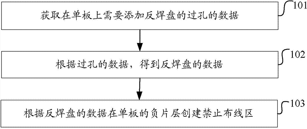
[0039] Embodiment 1, a method for setting vias on a single board, such as figure 1 shown, including:

[0040] Step S101: Obtain the data of the via holes on the single board that need to add anti-pads;

[0041] In an implementation manner of this embodiment, step S101 may specifically include:

[0042] Obtain the via information of all high-speed signal differential traces on the board;

[0043] Vias are highlighted for all high-speed signal differential traces.

[0044] Get the selected via in the highlighted via as the via to which the antipad needs to be added.

[0045] In other implementation manners, via holes that meet other predetermined conditions may also be used as via holes that need to be added with anti-pads.

[0046] Step S102: Obtain the data of the anti-pad according to the data of the via hole;

[0047] The data of the via hole may include, but is not limited to: the coordinates of the via hole, the radius of the via hole, and the like.

[0048] Optional...

Embodiment 2

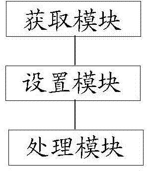
[0056] Embodiment 2, a device for setting via holes on a single board, such as figure 2 As shown, the device includes:

[0057] The acquisition module is used to acquire the data of the via holes that need to add anti-pads on the single board;

[0058] A setting module, configured to set the data of the anti-pad according to the data of the via hole;

[0059] The data of the via hole may include, but is not limited to: the coordinates of the via hole, the radius of the via hole, and the like.

[0060] The data of the anti-pad includes the radius of the anti-pad and the coordinates of the anti-pad.

[0061] In an implementation manner of this embodiment, the setting module sets the data of the anti-pad according to the data of the via hole may refer to:

[0062] The setting module sets the coordinates of the anti-pad as the coordinates of the via; according to the radius of the via, the size of the aperture of the anti-pad is set, and the radius of the anti-pad is obtained ...

Embodiment 3

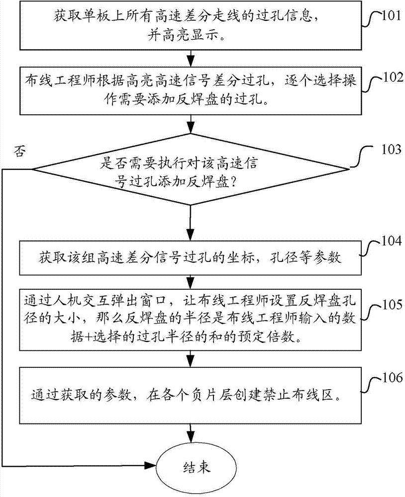
[0066] Embodiment three, such as image 3 As shown in the figure, taking a certain 16-layer CPU computing single board that needs anti-pad setting for a certain high-speed signal as an example, the above method of setting vias on a single board is explained in detail.

[0067]The 16-layer CPU computing board contains 8 negative layers. If you manually make anti-pads for each high-speed signal via, there will be a lot of repeated operations. If you use the above method, it only takes 2 to 3 seconds. , the time advantage is still very obvious.

[0068] Step S301: Obtain the via information of all high-speed signal differential traces on the single board, and display them in a highlighted manner.

[0069] Step S302: The wiring personnel select the vias that need to add anti-pads one by one according to the highlighted vias of the high-speed signal differential routing.

[0070] Step S303: judging whether it is necessary to add an anti-pad to the high-speed signal via hole.

[...


PUM


Abstract

The invention provides a method and device for arranging passing holes in a single plate. The method comprises the steps of obtaining the data of the passing holes of an anti-pad needing to be added to the single plate, obtaining the data of the anti-pad according to the data of the passing holes, and building a wiring forbidding area according to the data of the anti-pad. By means of the technical scheme, high-speed differential signals can be processed simply and rapidly, the design efficiency of the single plate can be largely improved, the impedance discontinuity degrees of the high speed signals, transmission loss of high-speed wiring of the single plate and the like are lowered, and the signal transmission quality is improved.

Description

technical field [0001] The present invention relates to the field of electronics, in particular, to a method and device for setting via holes on a single board. Background technique [0002] With the development of technology, the application of anti-pads in high-speed signals is becoming more and more important, especially in the R&D and design of large servers. In order to reduce the loss and impedance discontinuity of high-speed signal lines when changing layers, some processing is generally done on high-speed signals, that is, increasing the anti-pads of each layer of its reference plane to improve the transmission quality of its signals. However, it is quite cumbersome to make complex single-board anti-pads, and it is easy to miss. With the development of the current technology, the design of the single board becomes more and more complicated, and the environment of the high-speed wiring is relatively more and more harsh. The production of the anti-pad when the high-sp...

Claims


Application Information

Patent Timeline
Patent Type & Authority Applications(China)
IPC IPC(8): G06F17/50
Inventor 赵亚民李鹏翀
Owner 上海浪潮云计算服务有限公司
Why Eureka
Try Eureka