pop packaging structure and its packaging method

A packaging method and packaging structure technology, applied in electrical components, electrical solid devices, circuits, etc., can solve the problems of high cost, complicated and time-consuming implementation process, unfavorable packaging chips, etc., and achieve the effect of simplifying the manufacturing process and speeding up the processing time.

Active Publication Date: 2018-04-20
TSINGHUA UNIV
View PDF3 Cites 0 Cited by
  • Summary
  • Abstract
  • Description
  • Claims
  • Application Information

AI Technical Summary

Problems solved by technology

[0003] However, as mentioned above, in the existing POP manufacturing process, it is necessary to open holes on the plastic package and generate the second conductive terminal by solder printing. The implementation of these processes is complicated, time-consuming and costly.
Moreover, due to the limitation of hole opening technology, the first conductive terminal on the lower package body in the prior art can only be columnar or cone-shaped, which is not conducive to effectively utilizing the package area to obtain higher density and smaller area packages. chip

Method used


Image

  • pop packaging structure and its packaging method
  • pop packaging structure and its packaging method
  • pop packaging structure and its packaging method

Examples


Embodiment Construction

[0026] Specific embodiments of the present invention will be described in detail below in conjunction with the accompanying drawings. It should be understood that the specific embodiments described here are only used to illustrate and explain the present invention, and are not intended to limit the present invention.

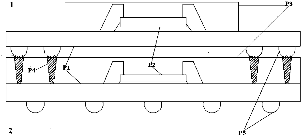
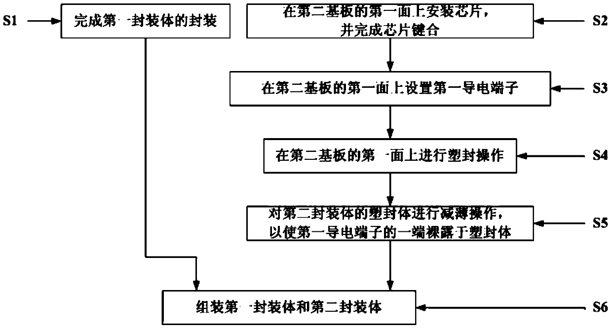
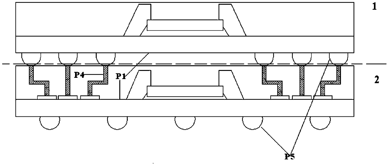
[0027] The present invention provides a packaging method for a POP packaging structure, the POP packaging structure includes a first package body and a second package body, the packaging method includes: mounting a chip on the first surface of a second substrate, and completing Chip bonding; setting a first conductive terminal on the pad on the first surface of the second substrate; performing a plastic encapsulation operation on the first surface of the second substrate to form a plastic package, the chip and the first conductive terminal are located in the plastic package; the plastic package of the second package is thinned, so that one end of the first condu...


PUM


Abstract

The invention discloses a POP packaging structure and a packaging method thereof. The packaging method includes the following steps that a chip is installed on the first face of a second substrate, and chip bonding is finished; a first electric conduction terminal is arranged on a bonding pad on the first face of the second substrate; plastic package operation is performed on the first face of the second substrate to form a plastic package body, and the chip and the first electric conduction terminal are located in the plastic package body; thinning operation is performed on the plastic package body of a second package body so that one end of the first electric conduction terminal can be exposed out of the plastic package body of the second package body; a first package body and the second package body are assembled. According to the POP packaging structure and the packaging method therefore, the technology difficulties such as laser etching hole filling and plastic package hole filling are avoided in the package process, and therefore the technology processes are simplified and processing time is shortened; special electric conduction terminals are convenient to achieve.

Description

technical field [0001] The invention relates to the field of integrated circuits, in particular to semiconductor package stacking. Background technique [0002] Package on Package (POP for short) is a typical semiconductor stack package, which refers to the stacking of two independently packaged packages. The schematic diagram of the traditional second-generation POP packaging structure is as follows figure 1 shown. Each package includes a substrate P1, a chip P2, a package P3 and a second conductive terminal P5. In order to assemble two independent packages 1 and 2, laser ablation is usually used to open a window at a specific position of the plastic package P3 of the lower package (also referred to herein as the second package) 2, and through The impurities are removed by chemical etching or plasma etching to expose the pads on the first surface of the second package 2 , and the hole formed in the plastic package P3 may be called a molded hole. Solder is then filled in...

Claims


Application Information

Patent Timeline
Patent Type & Authority Patents(China)
IPC IPC(8): H01L23/538H01L23/48H01L21/60H01L21/56
CPCH01L2224/73265
Inventor 陈瑜蔡坚王谦
Owner TSINGHUA UNIV
Why Eureka
Try Eureka