GaN-based light-emitting diode and manufacturing method thereof

A technology for light-emitting diodes and a manufacturing method, which is applied to electrical components, circuits, semiconductor devices, etc., can solve problems such as growth layer defects and affect the luminous efficiency of LEDs, and achieve the effect of ensuring crystal quality and improving luminous efficiency.

Active Publication Date: 2014-05-14
FOSHAN NATIONSTAR SEMICON
View PDF5 Cites 3 Cited by
  • Summary
  • Abstract
  • Description
  • Claims
  • Application Information

AI Technical Summary

Problems solved by technology

During the growth process of the quantum well active layer, defects in the growth layer appear and affect the luminous efficiency of LEDs. Therefore, how to improve the internal quantum efficiency of blue-green LEDs has become a research hotspot.

Method used


Image

  • GaN-based light-emitting diode and manufacturing method thereof
  • GaN-based light-emitting diode and manufacturing method thereof
  • GaN-based light-emitting diode and manufacturing method thereof

Examples


Embodiment Construction

[0072] As mentioned in the background section, the internal quantum efficiency of blue-green GaN-based LEDs in the prior art still needs to be improved.

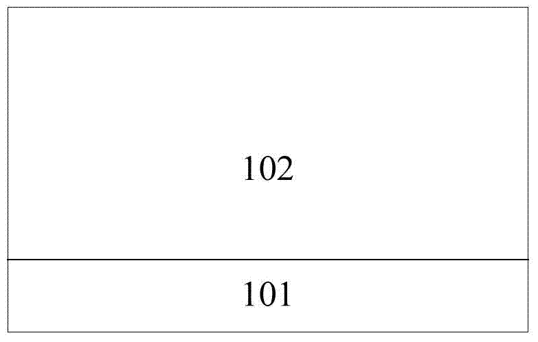
[0073] The inventors have found that the reason for the above phenomenon is that in traditional quantum wells, such as figure 1 As shown, including the well layer 101 and the barrier layer 102 located on the surface of the well layer, during the growth process of the active layer (well layer and barrier layer), along with the In x Ga 1-x N well layer or In y Ga 1-y With the growth of the N barrier layer, the thickness of the active layer increases, the distribution of In components in the well layer or barrier layer becomes uneven, and even at the end of the growth, In "agglomeration" will be formed at the next growth interface. In severe cases, In The nanoscale "ball" (In-droplet), the crystal quality of the next layer structure (well layer or barrier layer) grown under this interface will also deteriorate, which will af...


PUM

PropertyMeasurementUnit
Thicknessaaaaaaaaaa

Abstract

The invention provides a GaN-based light-emitting diode and a manufacturing method of the GaN-based light-emitting diode. A quantum well of the light-emitting diode comprises a well layer and a barrier layer. The well layer is an InxGa1-xN well layer, and the barrier layer is an InyGa1-yN barrier layer, wherein y<x<1, 0<x<1 and 0<=y<1. At least one GaN tunneling layer is arranged in the well layer and / or the barrier layer. Due to the fact that the GaN tunneling layer is added, before the well layer or the barrier layer grows to a certain thickness and In gathering occurs, the GaN tunneling layer is grown, and therefore the In gathering phenomenon of the well layer and / or the barrier layer is avoided. The crystalline quality of the quantum well is improved, and therefore the light-emitting efficiency of the light-emitting diode is improved.

Description

technical field [0001] The invention relates to the technical field of manufacturing semiconductor devices, in particular to a GaN-based light-emitting diode and a manufacturing method thereof. Background technique [0002] Light-Emitting Diode (LED for short) has the advantages of high brightness, low energy consumption, long life, and fast response speed. There are a wide range of applications. With the development of light-emitting diodes, GaN-based light-emitting diodes have become mainstream products in the market. [0003] Moreover, the current market demand for blue-green LEDs is increasing, and the performance requirements for blue-green LEDs are also getting higher and higher. At present, the quantum well active layer of blue-green LED is generally In x Ga 1-x N / In y Ga 1-y N, where In x Ga 1-x In composition x in N well layer is greater than In y Ga 1-y In composition y in the N barrier layer. During the growth process of the quantum well active layer, d...

Claims


Application Information

Patent Timeline
IPC IPC(8): H01L33/06H01L33/32H01L33/00
CPCH01L33/0075H01L33/06H01L33/145H01L33/32
Inventor 张冀李鹏
Owner FOSHAN NATIONSTAR SEMICON
Why Eureka
Try Eureka