
Novel ceramic capacitor

A technology of ceramic capacitors and ceramics, applied in fixed capacitor electrodes, fixed capacitor leads, fixed capacitor shells/packages, etc., can solve the problems of ceramic capacitors with reduced insulation resistance, inability to mold, low production efficiency, etc., to avoid insulation resistance The effect of falling, good insulation of water vapor, and simple structure

Inactive Publication Date: 2014-05-21
CHENGDU RONGHUA ELECTRONICS
View PDF3 Cites 2 Cited by
  • Summary
  • Abstract
  • Description
  • Claims
  • Application Information

AI Technical Summary

Problems solved by technology

Ceramic capacitors with this structure cannot be molded due to the different heights of the circular cross-section pins during production, so they can only be soldered and packaged individually, and the production efficiency is low.
Most ceramic capacitors use epoxy resin to encapsulate the surface. The epoxy resin encapsulation layer is cured to form a shell. The epoxy resin encapsulation layer encapsulates the ceramic chip, electrodes and some pins, and the surface is encapsulated with epoxy resin. To a certain extent, the withstand voltage and insulation properties of ceramic capacitors can be improved, but due to the characteristics of epoxy resin itself, many through-hole pores will remain after curing, so ceramic capacitors are easy to Moisture, water vapor enters the interior of the ceramic chip, resulting in a decrease in the insulation resistance of the ceramic capacitor, poor voltage resistance, and easy burnout
In addition, small computers, mobile communications and other equipment are becoming lighter, thinner, shorter, and smaller, and the requirements for performance and functions are becoming more and more stringent. There is a greater demand for ceramic capacitors with small volume and large capacity, which requires a higher dielectric constant. Ceramic capacitors, but the higher the dielectric constant, the larger the volume of ceramic capacitors, which is not suitable for use in small communication devices such as mobile phones and handheld computers.

Method used


Image

  • Novel ceramic capacitor

Examples


Embodiment Construction

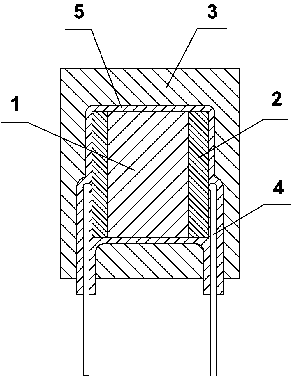
[0009] As an embodiment of the present invention, such as figure 1 As shown, a novel ceramic capacitor includes a ceramic chip 1, the ceramic chip 1 is in the shape of a cuboid, and tin electrodes 2 are respectively fixedly connected to the opposite sides of the ceramic chip 1, and the use of the tin electrode 2 can increase the size of the ceramic capacitor. The dielectric constant makes the ceramic capacitor produce a large capacitance in the case of a small volume, and give full play to the stability and reliability of the capacitor. It is suitable for application in small communication devices such as mobile phones and palmtop computers. The ceramic chip 1 and the tin electrode 2 are provided with an epoxy resin encapsulation layer 3, and the two tin electrodes 2 are respectively provided with a pin 4, and the cross section of the pin 4 is rectangular, so that the pin 4 of the ceramic capacitor can Located at the same height, during production, multiple ceramic capacitors...


PUM

PropertyMeasurementUnit
thicknessaaaaaaaaaa

Abstract

The invention discloses a novel ceramic capacitor and relates to an electronic component. The novel ceramic capacitor comprises a rectangular ceramic chip, a tin electrode is firmly connected with each of two opposite lateral surfaces of the ceramic chip, an epoxy resin packing layer is mounted at the outside of each of the ceramic chip and the tin electrodes, a pin is mounted on each of two tin electrodes, the cross section of each pin is rectangular, one end of each pin is firmly connected with the tin electrodes while the other end extends out of the epoxy resin packing layer, and a paint layer is respectively arranged between the ceramic chip and the epoxy resin packing layer, between the tin electrodes and the epoxy resin packing layer, and between the pins and the epoxy resin packing layer. The novel ceramic capacitor is simple in structure, is reasonable in design, is convenient to process, is capable of greatly improving the production efficiency, is large in capacitance, is suitable for such small communication equipments as mobile phone and palm computer, has good humidity resistance and is capable of preventing the outside water entering the ceramic chip in the ceramic capacitor so that the insulation resistance decrease and the undesirable voltage resistance of the ceramic capacitor due to moisture are avoided, and is practical.

Description

technical field [0001] The invention relates to an electronic component, in particular to a novel ceramic capacitor. Background technique [0002] A ceramic capacitor is a capacitor with ceramic as a dielectric. The existing ceramic capacitor generally includes a ceramic chip, a pin and an epoxy resin encapsulation layer. The cross section of the existing pin is circular. During the production of ceramic capacitors with this structure, because the pins with circular cross-sections have different heights, they cannot be molded, so they can only be soldered and packaged individually, and the production efficiency is low. Most ceramic capacitors use epoxy resin to encapsulate the surface. The epoxy resin encapsulation layer is cured to form a shell. The epoxy resin encapsulation layer encapsulates the ceramic chip, electrodes and some pins, and the surface is encapsulated with epoxy resin. To a certain extent, the withstand voltage and insulation properties of ceramic capacito...

Claims


Application Information

Patent Timeline
Patent Type & Authority Applications(China)
IPC IPC(8): H01G4/008H01G4/224H01G4/228
Inventor 李应忠
Owner CHENGDU RONGHUA ELECTRONICS
Learn More