Clock-feedthrough compensation method of bootstrap clock sampling switch and circuit

A technology of clock feedthrough and clock sampling, applied in the field of circuits

Active Publication Date: 2014-05-28
XIAMEN UX HIGH SPEED IC
View PDF3 Cites 5 Cited by
  • Summary
  • Abstract
  • Description
  • Claims
  • Application Information

AI Technical Summary

Problems solved by technology

[0004] For the crosstalk error caused by the bootstrap clock feedthrough through the gate-to-drain parasitic capacitance, the gate voltage bootstrap switch is usually used to eliminate the crosstalk error, so that the gate voltage of the sampling switch and the gate voltage of the dummy switch are provided by the gate voltage bootstrap switch; The limitation of the method is that the gate voltage of the introduced dummy switch is biased to Vin+Vdd during the holding phase, because Vin is changing, so the changing gate voltage will also interfere with the sampling value through the parasitic Cgd capacitive coupling

Method used


Image

  • Clock-feedthrough compensation method of bootstrap clock sampling switch and circuit
  • Clock-feedthrough compensation method of bootstrap clock sampling switch and circuit

Examples


Embodiment Construction

[0042] The present invention will be further described below in conjunction with drawings and embodiments.

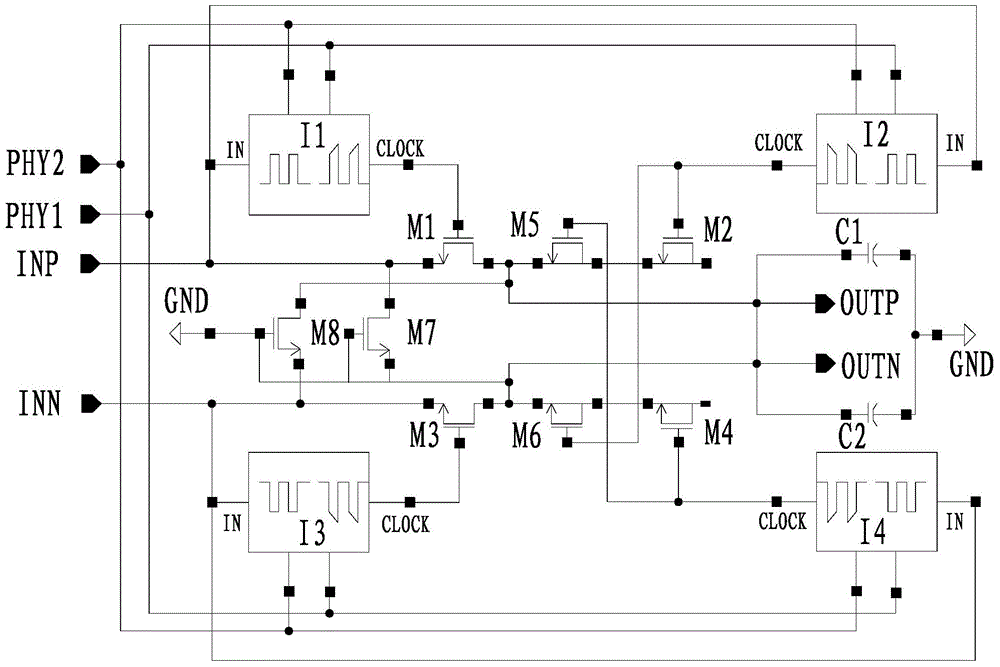
[0043] refer to figure 1 , a clock feedthrough compensation circuit for a bootstrap clock sampling switch, comprising:

[0044]The first sampling transistor M1, the gate of the first sampling transistor M1 is connected to the clock output terminal of the first gate voltage bootstrap circuit I1, the source of the first sampling transistor M1 is connected to the first differential complementary signal INP, The drain of the first sampling transistor M1 is connected to the first output terminal OUTP;

[0045] A first dummy switch transistor M2, the gate of the first dummy switch transistor M2 is connected to the clock output end of the second gate voltage bootstrap circuit I2;

[0046] A first storage capacitor C1, one end of the first storage capacitor C1 is connected to the first output terminal OUTP; the other end of the first storage capacitor C1 is connected to GND; ...


PUM


Abstract

The invention provides a clock-feedthrough compensation method of a bootstrap clock sampling switch. New pseudo switches are added at sampling output nodes, the grid electrodes of the new pseudo switches are biased at the clock output end of a complementary grid voltage bootstrap circuit, error amount generated when the newly-added pseudo switches and the original pseudo switches are coupled onto Vout via Cgd can be mutually offset. The invention provides a clock-feedthrough compensation circuit of the bootstrap clock sampling switch which is designed by the above method. Preferably, a group of pseudo switches in a switching off state is introduced, in the sample and hold stage, the complementary input signals are coupled on Vout respectively via a parasitic Cds capacitor, and cross talk can be mutually offset as the input signals are complementary. The clock-feedthrough compensation circuit of the bootstrap clock sampling switch has the advantages of reducing the influences of the clock-feedthrough effect on signal sampling, improving linearity of a sampling field effect tube, reducing harmonic distortion of the sampling circuit, and improving the sampling speed and the sampling precision.

Description

technical field [0001] The invention relates to a circuit, in particular to a clock feedthrough compensation circuit for a bootstrap clock sampling switch. Background technique [0002] In the ADC (Analog to Digital Converter, analog-to-digital converter) circuit system, a sample and hold circuit (sample and hold) is often used, and its function is to collect the instantaneous value of the analog input voltage at a certain moment, and convert the The output voltage is kept constant during the converter conversion for analog-to-digital conversion. When the level is high, the switch is closed, and the output follows the input signal. When the level is low, the switch is turned off, and the holding capacitor keeps the output voltage constant. [0003] In the actual circuit, the sampling error caused by the parasitic capacitance of the switching device and the charge injection effect mainly includes: 1. The crosstalk error caused by the parasitic source-drain capacitance 2. The...

Claims


Application Information

Patent Timeline
Patent Type & Authority Applications(China)
IPC IPC(8): H03M1/54
Inventor 林少衡
Owner XIAMEN UX HIGH SPEED IC
Why Eureka
Try Eureka