Wafer detection device and method used for ashing machine

A detection method and detection device technology, which are used in measurement devices, optical testing flaws/defects, semiconductor/solid-state device testing/measurement, etc., to achieve the effect of reducing the number of scraps and prolonging service life

Inactive Publication Date: 2014-06-04
SHANGHAI HUAHONG GRACE SEMICON MFG CORP
View PDF6 Cites 3 Cited by
  • Summary
  • Abstract
  • Description
  • Claims
  • Application Information

AI Technical Summary

Problems solved by technology

[0005] However, the above-mentioned ashing machine generally does not detect the state of the processed wafer 30 in the reaction chamber 10 before extending the vacuum arm 20

Method used


Image

  • Wafer detection device and method used for ashing machine
  • Wafer detection device and method used for ashing machine
  • Wafer detection device and method used for ashing machine

Examples


Embodiment Construction

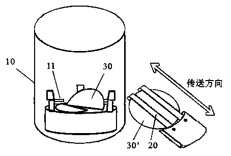
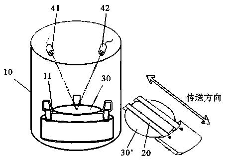
[0020] Such as figure 2 As shown, the wafer detection device used in the ashing machine according to the present invention is used to detect the state of the wafer 30 before transferring the processed wafer 30 in the reaction chamber 10 .

[0021] The wafer detection device includes an infrared transmitter 41 and a corresponding receiver 42, which are respectively arranged on the top in the reaction chamber 10 and above the wafer 30; then, if the infrared rays produced by the transmitter 41, If the normal reflection from the surface of the wafer 30 reaches the receiver 42 , it means that the wafer 30 is complete, and the vacuum arm 20 can be controlled to extend into the reaction chamber 10 to pick up the wafer 30 .

[0022] If the wafer 30 in the reaction chamber 10 is damaged, it may be that the emitted infrared rays cannot reach the surface of the wafer 30, or the angle at which the infrared rays are reflected by the wafer 30 may change, so that the infrared rays cannot no...


PUM


Abstract

The invention relates to a wafer detection device and method used for an ashing machine. The method includes: before a vacuum arm is used to transport a wafer which is processed in a reaction chamber, whether the wafer is broken is detected; infrared ray is firstly sent by an emitter to the surface of the wafer and if infrared ray reflected by the wafer can be received by a receiver, it proves that the wafer is not broken and then the vacuum arm is controlled to extend out into the reaction chamber to replace the wafer; and if the receiver cannot receive the infrared ray, it proves that the wafer is broken and then the vacuum arm is stopped from continuing to extend out. The wafer detection device and method are simple and reliable and capable of detecting conveniently the state of the wafer before the wafer is transported so that after the wafer is found to be broken, the vacuum arm can be stopped immediately from extending out into the reaction chamber and thus the number of scrapped wafers is reduced and the vacuum arm and lift pins in the reaction chamber are protected and the service life of the machine is prolonged.

Description

technical field [0001] The invention relates to the field of semiconductors, in particular to a wafer detection device and method for an ashing machine. Background technique [0002] Such as figure 1 As shown, a machine for photoresist ashing process of KEM Company is taken as an example. [0003] Cooperate see image 3 As shown, several lift pins 11 (lift pins) in the reaction chamber 10 are evenly distributed along the circumference, and are used to replace two wafers 30 and 30' in cooperation with a vacuum arm 20 (vacuum arm). These ejector pins 11 have four working positions in the vertical direction, which are respectively: bottom A1, low position A2, middle position A3, and high position A4. The vacuum arm 20 further includes an upper arm 21 and a lower arm 22 , the upper arm 21 and the lower arm 22 do not change their positions in the vertical direction, but only move in and out of the reaction chamber 10 in the horizontal direction. The vertical position of the u...

Claims


Application Information

Patent Timeline
IPC IPC(8): H01L21/67H01L21/66G01N21/88
CPCH01L21/67259G01N21/9501
Inventor 吴红帅吴敏
Owner SHANGHAI HUAHONG GRACE SEMICON MFG CORP
Why Eureka
Try Eureka