
Multilayer wiring substrate and manufacturing method thereof

A multilayer wiring substrate and manufacturing method technology, applied in the directions of multilayer circuit manufacturing, printed circuit manufacturing, printed circuit stress/deformation reduction, etc., can solve problems such as inability to obtain surface roughness, decrease in bonding strength of conductor layers, etc., to achieve Excellent connection reliability, suppression of thermal expansion coefficient, and effects of stress relaxation

Inactive Publication Date: 2014-06-04
NGK SPARK PLUG CO LTD
View PDF5 Cites 4 Cited by
  • Summary
  • Abstract
  • Description
  • Claims
  • Application Information

AI Technical Summary

Problems solved by technology

However, when the particle size of the silica filler is reduced, sufficient surface roughness cannot be obtained even if the surface of the resin insulating layer is roughened, and the adhesion strength of the conductor layer ensured by the anchoring effect decreases.

Method used


Image

  • Multilayer wiring substrate and manufacturing method thereof
  • Multilayer wiring substrate and manufacturing method thereof
  • Multilayer wiring substrate and manufacturing method thereof

Examples


Embodiment Construction

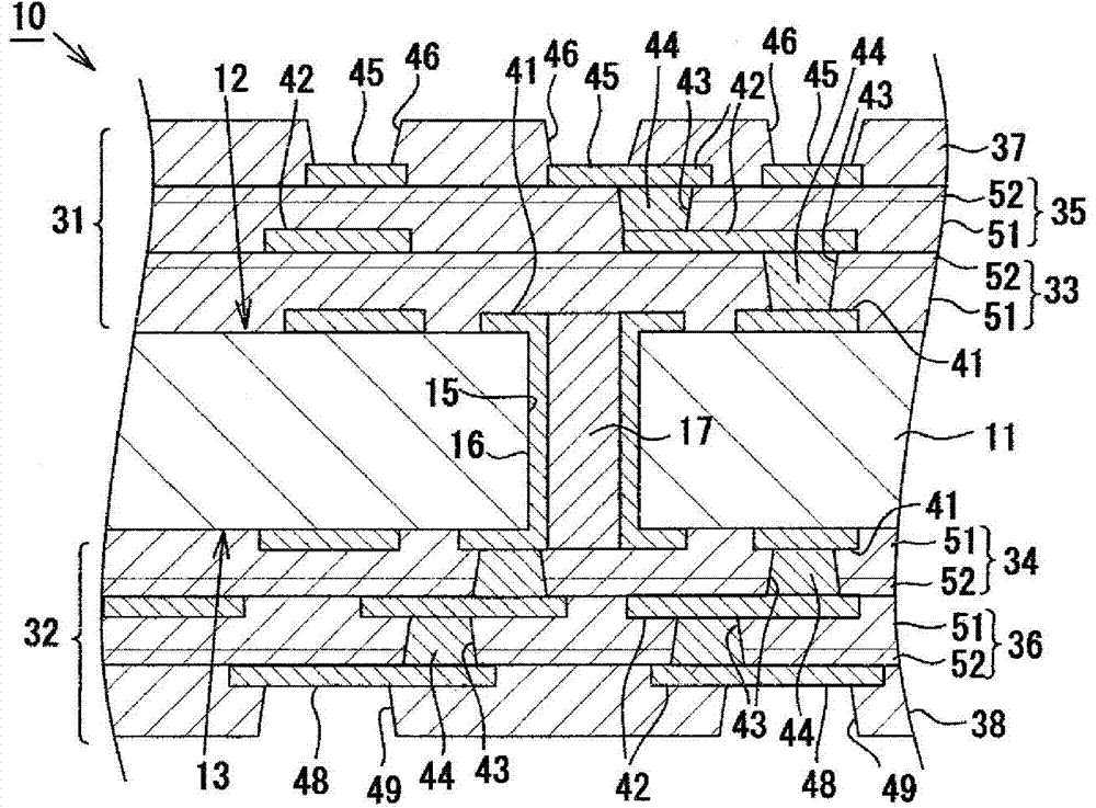
[0030] Hereinafter, an embodiment embodying the present invention as a multilayer wiring board will be described in detail with reference to the drawings.

[0031] Such as figure 1 As shown, the multilayer wiring board 10 of this embodiment includes a core substrate 11, and a core main surface 12 (in the figure 1 The middle is the upper surface) on the first build-up layer 31, and the core back surface 13 (in the figure 1 The middle is the second build-up layer 32 on the lower surface.

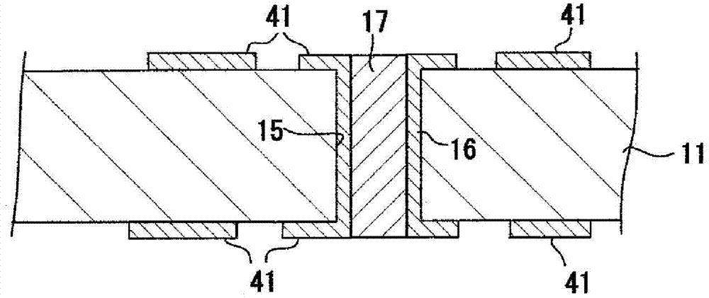
[0032] The core substrate 11 is composed of, for example, a resin insulating material (glass epoxy material) obtained by impregnating glass fiber cloth as a reinforcing material with epoxy resin. Conductive holes 15 (through holes) penetrating the core substrate 11 in the thickness direction are formed in a plurality of locations of the core substrate 11, and conductive conductors 16 are formed in the conductive holes 15. The via conductor 16 connects the core main surface 12 side and the core b...


PUM


Abstract

Provided is a multilayer wiring substrate capable of sufficiently ensuring adhesion between resin insulation layers and conductor layers and which has excellent connection reliability. This multilayer wiring substrate (10) has a multilayer build-up structure comprising multiple resin insulation layers (33-36) and multiple conductor layers (42) laminated alternately. The resin insulation layers (33-36) comprise a lower insulation layer (51) and an upper insulation layer (52) provided on the lower insulation layer (51), and on the surface of the upper insulation layer (52) is formed a conductor layer (42). The upper insulation layer (52) is formed thinner than the lower insulation layer (51), and the volume ratio of the silica filler in the upper insulation layer (52) is less than the volume ratio of the silica filler and glass cloth in the lower insulation layer (51).

Description

Technical field [0001] The present invention relates to a multilayer wiring board having a multilayer structure in which a plurality of resin insulating layers and a plurality of conductor layers are alternately laminated to be multilayered, and a method of manufacturing the same. Background technique [0002] In recent years, with the miniaturization of electrical equipment, electronic equipment, etc., there has also been a demand for miniaturization and high density of multilayer wiring boards mounted on these equipment. As this multilayer wiring board, a wiring board manufactured by a so-called build-up method (Japanese: ビルドアップ method) in which a plurality of resin insulating layers and a plurality of conductor layers are alternately laminated and integrated is used. In addition, in such a multilayer wiring board, for the purpose of improving the adhesion between the resin insulating layer and the conductor layer formed by plating on the resin insulating layer, or for the purp...

Claims


Application Information

Patent Timeline
IPC IPC(8): H05K3/46H01L23/12H01L23/14
CPCH01L2924/0002H01L23/145H05K1/036H05K2201/0195H01L23/49822H05K2201/068H05K1/0373H05K3/4673H01L23/49827H01L23/49894H01L23/3735H01L23/3737Y10T29/49162H01L2924/00H05K1/0271H05K1/0306
Inventor 前田真之介
Owner NGK SPARK PLUG CO LTD
Learn More